Silicide thin-film deposition is not just about choosing the right metal silicide. Phase formation, deposition methods, and annealing conditions can directly affect film resistivity, uniformity, and interface quality. This guide compares sputtering, salicide, and chemical vapor deposition (CVD), and explains how TiSi₂ phase transformations and material selection influence thin-film performance.
1. What Is Silicide Thin-Film Deposition?
Silicides are compounds formed between silicon and metals such as titanium, nickel, cobalt, tungsten, and molybdenum. They are used in electronic materials, semiconductor processing, conductive layers, and high-temperature applications.
In semiconductor technology, metal silicides have been investigated and used to reduce contact and interconnect resistance. Their performance depends on factors such as chemical composition, crystal structure, film thickness, interface condition, and thermal history.
Common silicide systems include:
| Silicide | Typical material or process relevance |
| Titanium disilicide (TiSi₂) | Historically important for low-resistance contacts and interconnect applications |
| Cobalt disilicide (CoSi₂) | Used in semiconductor contact and interface research |
| Nickel disilicide (NiSi₂) | A distinct nickel–silicon phase with different structural and electrical characteristics |
| Tungsten disilicide (WSi₂) | Used in high-temperature materials and certain semiconductor processing systems |
| Molybdenum disilicide (MoSi₂) | Known for high-temperature oxidation-resistant applications and functional coatings |
For a broader overview of available deposition materials, see ULPMAT’s thin-film deposition materials, which include metal, alloy, and ceramic sputtering targets as well as evaporation materials.
2. Which Silicide Phases Matter for Thin-Film Properties?
The phase composition of a silicide film can influence its electrical resistivity, microstructure, and stability during subsequent processing.
This is particularly important in titanium silicide systems. TiSi₂ can form in two commonly discussed phases:
C49-TiSi₂: A metastable phase that may form during early stages of reaction between titanium and silicon.
C54-TiSi₂: The thermodynamically stable phase under relevant processing conditions and generally associated with lower electrical resistivity than C49-TiSi₂.
The transformation from C49 to C54 is therefore an important consideration in processes where low-resistance titanium silicide is required.
However, phase formation is not determined by temperature alone. Film thickness, silicon substrate orientation, microstructure, impurities, interface condition, and annealing history can all affect the transformation.
Other metal–silicon systems have their own phase diagrams and reaction pathways. The TiSi₂ C49-to-C54 transformation should not be generalized to every silicide material.
How can silicide phases be evaluated?
X-ray diffraction (XRD) is commonly used to identify crystalline phases and investigate phase evolution during processing. Depending on the film and application, additional methods may be needed:
Four-point probe: Measures sheet resistance and helps evaluate electrical changes during annealing.
Scanning electron microscopy (SEM): Examines surface morphology, grain structure, and possible agglomeration.
Transmission electron microscopy (TEM): Provides detailed information about interfaces, grain structures, and nanoscale phases.
Energy-dispersive X-ray spectroscopy (EDS): Helps examine elemental distribution and local composition.
No single measurement provides a complete picture. Phase identification, electrical characterization, and microstructural analysis are most useful when interpreted together.
3. Why Does the C49-to-C54 Transformation Matter in TiSi₂ Films?
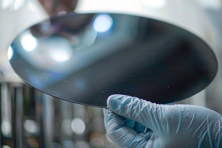
The C49-to-C54 transformation is one of the best-known examples of phase control in silicide thin-film processing.
C49-TiSi₂ may form first during the reaction between deposited titanium and silicon. Further thermal treatment can promote the formation of C54-TiSi₂, which is generally preferred where lower resistivity is required.
In conventional Ti/Si reaction systems, the transformation is often discussed within an approximate temperature range of 700–900°C. This range is a general reference rather than a universal process specification. Published studies have reported different transformation conditions depending on film thickness, substrate orientation, and experimental setup. Some specialized processes have also achieved C54 formation at lower temperatures.
Several factors should be considered:
Film thickness: Thin films may exhibit different phase-transformation behavior from thicker films. Thickness-dependent changes can also affect measured resistivity.
Substrate orientation: The crystallographic orientation of silicon can influence nucleation and phase formation.
Microstructure: Grain size, interface structure, and defects can affect the development of the final silicide phase.
Impurities and contamination: Unwanted elements or surface contamination may interfere with interfacial reactions and film uniformity.
Annealing conditions: Temperature, holding time, heating rate, and atmosphere all influence reaction progress and phase evolution.
Excessive thermal exposure can also create other problems, including grain growth, film agglomeration, or degradation of the interface. The objective is therefore not simply to increase the annealing temperature, but to identify a process window that produces the required phase while maintaining film continuity and electrical performance.
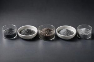
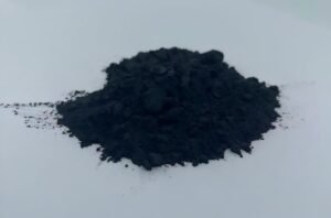
For researchers working with titanium silicide starting materials, ULPMAT provides Titanium Silicide Powder (TiSi₂). The listed specification includes 99.5% purity and -325 mesh. Powder specifications should be evaluated separately from the requirements for a deposited film or a finished sputtering target.
4. Which Silicide Film Formation Route Should You Choose?
Silicide thin films can be produced through different routes. The most suitable method depends on the material system, substrate, film requirements, and available process equipment.
4.1 Sputtering from a Silicide Target
Sputtering is a physical vapor deposition (PVD) technique in which energetic ions bombard a solid target and eject material species. These species travel through the vacuum chamber and deposit onto a substrate, gradually forming a thin film.
When a silicide target is used, the target composition provides the starting material for deposition. However, the composition and phase of the deposited film should not automatically be assumed to match the target exactly. Preferential sputtering, process conditions, substrate temperature, and post-deposition treatment can influence the final film.
Important process variables include:
Sputtering power and power density
Working pressure and process gas conditions
Target-to-substrate distance
Substrate temperature
Deposition rate and film thickness
Substrate surface condition
Post-deposition annealing
Target material selection should therefore be considered together with the deposition process and the intended film properties.
You can explore ULPMAT’s Metal Sputtering Targets, Alloy Sputtering Targets, and Ceramic Sputtering Targets to understand the different material categories used in PVD systems.
For a broader explanation of target materials and deposition principles, see our article on the TCO Manufacturing Process, which discusses the relationship between powder preparation, target fabrication, thin-film deposition, and film characterization.
4.2 Salicide Processing
Salicide, short for self-aligned silicide, is a process used in semiconductor fabrication.
In a typical salicide process, a metal layer is deposited over a silicon-containing structure. During subsequent thermal treatment, the metal reacts with exposed silicon to form a metal silicide. Unreacted metal is then removed from regions where the reaction has not occurred, depending on the process sequence.
The self-aligned nature of the reaction allows silicide to form selectively on exposed silicon or polysilicon regions.
The process is sensitive to several factors:
Metal thickness and deposition uniformity
Silicon surface condition
Reaction temperature and time
Phase formation and transformation
Unwanted lateral reaction or bridging
Agglomeration and interface stability
The appropriate metal and process conditions depend on the device structure and technology generation. A process developed for one silicide system should not be transferred directly to another without validation.
4.3 Chemical Vapor Deposition (CVD) and Polycide Structures
Chemical vapor deposition introduces gaseous precursors that react or decompose at a substrate surface to form a solid film.
In semiconductor processing, CVD has been used to deposit tungsten silicide layers on polysilicon, forming polycide structures. Such structures combine polysilicon with a silicide layer to modify electrical properties.
CVD and sputtering differ in their material delivery mechanisms. CVD depends on precursor chemistry, gas transport, surface reactions, and reaction conditions, while sputtering relies on the physical ejection and transport of material from a target.
The choice between them depends on film composition, conformality requirements, substrate geometry, process integration, and available equipment.
5. How Do Annealing Conditions Affect Silicide Film Formation?
Annealing is often used to promote reactions, modify crystal structure, and influence the electrical properties of silicide films.
However, the response to annealing varies significantly among material systems. A suitable thermal process for TiSi₂ may not be suitable for NiSi, CoSi₂, or WSi₂.
The main variables include:
Temperature: Determines the thermodynamic and kinetic conditions for phase formation and transformation.
Holding time: Influences how far a solid-state reaction proceeds. Longer treatment does not always improve the final film.
Atmosphere: Vacuum, inert gas, or other controlled environments may be selected depending on the material and process requirements. Uncontrolled oxidation can alter the film or interface.
Heating and cooling rates: Can influence nucleation, grain growth, and the development of different phases.
Substrate and interface: The substrate composition, surface preparation, and interface condition can affect reaction kinetics and film stability.
A practical evaluation should combine structural and electrical measurements. XRD can help identify phase changes, while sheet-resistance measurements can show whether the electrical properties change as expected. SEM or TEM can provide additional information when morphology or interface degradation is suspected.
The best annealing condition is the one that achieves the required phase and electrical performance without causing unacceptable agglomeration, diffusion, or loss of film continuity.
6. Common Silicide Thin-Film Problems and What to Check
Silicide films can show different types of defects during deposition or thermal processing. The first step in troubleshooting is to identify whether the problem originates from the starting material, deposition process, substrate, or post-deposition treatment.
| Observed problem | Possible factors to investigate |
| Higher-than-expected resistivity | Phase composition, film thickness, impurities, grain structure, and interface quality |
| Nonuniform film composition | Target composition, preferential sputtering, process stability, and substrate position |
| Film agglomeration | Excessive thermal exposure, film thickness, surface energy, and substrate condition |
| Poor thickness uniformity | Target geometry, deposition configuration, substrate movement, and process parameters |
| Unexpected crystalline phases | Reaction temperature, annealing time, starting composition, and contamination |
| Interface degradation | Surface preparation, thermal budget, diffusion, and interfacial reactions |
| Batch-to-batch variation | Starting material consistency, target condition, equipment history, and process repeatability |
These are investigation points rather than universal explanations. For example, high resistivity does not necessarily indicate a target-quality problem. It may result from the deposited film’s phase, thickness, microstructure, or interface.
Similarly, a composition difference between a target and a film does not automatically indicate a defective target. Deposition conditions and material-dependent sputtering behavior should also be examined.
A useful troubleshooting sequence is:
Confirm the chemical composition and material identity.
Review target or source-material condition.
Check deposition records and process stability.
Measure film thickness and sheet resistance.
Identify crystalline phases using XRD where appropriate.
Examine surface and interface morphology if the initial results indicate structural problems.
Compare results across batches and process runs.
For broader information about sputtering target selection and quality considerations, visit ULPMAT’s sputtering target product categories.
7. How to Select Silicide Sputtering Targets
When sputtering is selected as the deposition route, the target should be evaluated according to the requirements of the intended film and deposition system.
Chemical composition
Confirm the target’s nominal formula and elemental ratio. For compound materials, the stoichiometric ratio is particularly important because composition can influence phase formation and film properties.
Purity and impurities
The required purity depends on the application. Trace impurities may influence electrical behavior, phase formation, or film reliability, particularly in sensitive electronic applications.
Ask for available composition information and supporting documentation rather than relying on a nominal purity value alone.
Phase composition
Where crystalline phase is important, clarify whether the target’s phase composition is specified or characterized. Also consider whether the deposited film is expected to undergo phase changes during subsequent processing.
Density and microstructure
Target density, porosity, and microstructural uniformity can influence mechanical integrity and sputtering behavior. The appropriate requirements depend on the material, target dimensions, and equipment configuration.
Geometry and dimensions
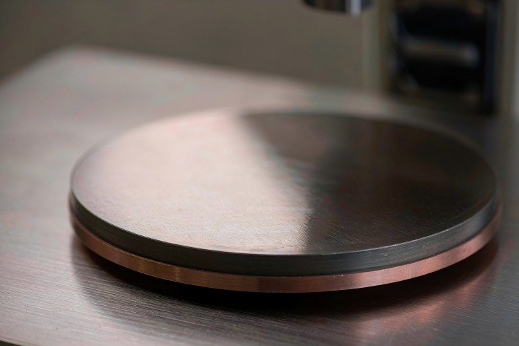
The target must be compatible with the sputtering system. Confirm dimensions, shape, thickness, mounting requirements, and whether a backing plate is needed.
Bonding and documentation
For bonded targets, clarify the bonding configuration and relevant inspection or documentation requirements. Available documents may include a certificate of analysis (COA), technical data sheet (TDS), and other quality records, depending on the product and order.
Before finalizing a specification, communicate the intended deposition process, target dimensions, substrate, and film requirements to the supplier.
8. From Silicide Powder to Sputtering Target
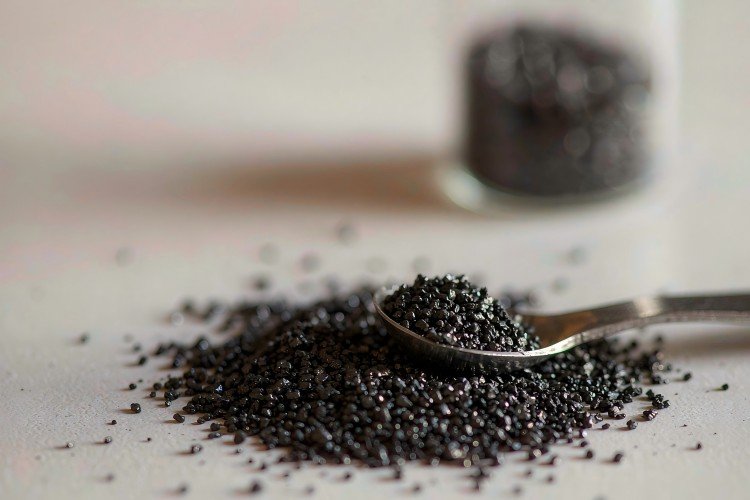
Powder characteristics can influence the preparation of a sputtering target, but powder specifications alone do not establish the quality of a finished target.
A typical powder-metallurgy route may involve several stages:
Raw material selection: Confirm chemical composition, purity, and the required silicide phase.
Powder preparation: Evaluate particle size, morphology, oxygen content, and potential contamination.
Mixing and forming: Prepare the powder and form it into a suitable compact, depending on the material and production route.
Densification: Apply an appropriate consolidation or sintering process.
Machining and finishing: Produce the required target geometry and surface condition.
Inspection: Evaluate relevant properties such as dimensions, density, composition, and structural uniformity.
The actual process depends on the material’s melting behavior, oxidation sensitivity, phase stability, and consolidation characteristics. Not every silicide can be processed using the same manufacturing parameters.
For this reason, buyers should distinguish between a silicide powder specification and a finished sputtering target specification. A powder with a stated purity and mesh size does not automatically guarantee a target with a particular density, bonding quality, or sputtering performance.
9. Silicide Materials Available from ULPMAT
ULPMAT supplies inorganic powders and thin-film deposition materials for research and industrial material development. Its product range includes silicide powders as well as metal, alloy, and ceramic sputtering targets.
The following silicide powder pages provide examples of listed materials and specifications:
Titanium Silicide Powder (TiSi₂) – listed at 99.5% purity and -325 mesh.
Tungsten Silicide Powder (WSi₂) – listed specifications include 99% at -200 mesh and 99.5% at -325 mesh.
Niobium Silicide Powder (NbSi₂) – listed at 99% and 99.5% purity, both at -325 mesh.
Nickel Silicide Powder (NiSi₂) – listed specifications include 99% at -80 mesh and 99.5% at -325 mesh.
Magnesium Silicide Powder (Mg₂Si) – listed at 99% purity and -200 mesh.
These are powder products, not a statement that each material is available as a sputtering target. Target availability, dimensions, composition, and processing requirements should be confirmed separately.
To learn more about ULPMAT’s material range and business, visit About ULPMAT. For questions about material specifications, product availability, or customization, you can also review the ULPMAT FAQs or contact the ULPMAT team.
FAQs
Silicide sputtering deposits material from a solid target onto a substrate through a physical vapor deposition process. Salicide forms a silicide through a reaction between a deposited metal and exposed silicon during thermal processing. The two methods use different material formation mechanisms.
C49-TiSi₂ is a metastable phase, while C54-TiSi₂ is the stable phase generally associated with lower resistivity. The transformation can therefore be important when low-resistance titanium silicide is required. Its conditions depend on film thickness, substrate orientation, microstructure, and thermal history.
No. NiSi is nickel monosilicide, while NiSi₂ is nickel disilicide. They are distinct compounds with different phase characteristics and should be specified separately when selecting materials or interpreting thin-film results.
Not necessarily. The deposited film can be influenced by preferential sputtering, process conditions, substrate temperature, and post-deposition reactions. Film composition should be verified when it is critical to the application.
XRD is useful for crystalline phase identification. Four-point probe measurements can evaluate sheet resistance, while SEM and TEM can help examine morphology and interfaces. EDS can provide information about elemental distribution. The appropriate combination depends on the film and the property being investigated.
Not usually without further processing. Powder must be consolidated into a target with suitable dimensions, density, mechanical integrity, and other application-specific properties. Powder purity and particle size are only part of the overall target specification.
Conclusion
Silicide thin-film performance depends on the relationship between material composition, deposition route, phase formation, and thermal processing. Sputtering, salicide, and CVD offer different approaches to forming silicide-containing layers, and each requires process conditions suited to the material system.
For TiSi₂, the C49-to-C54 transformation illustrates why phase control can be as important as nominal chemical composition. More generally, reliable evaluation should combine material specifications with film-level characterization, including phase identification, electrical measurements, and microstructural analysis.
When selecting silicide materials or sputtering targets, consider the intended deposition route, composition, phase requirements, substrate compatibility, and available quality documentation. These factors provide a more practical basis for evaluating material suitability than purity or nominal formula alone.
References
- 1. Jeon, H., Yoon, G., and Nemanich, R. J. “Dependence of the C49–C54 TiSi₂ Phase Transition Temperature on Film Thickness and Si Substrate Orientation.” Thin Solid Films, 299(1–2), 178–182 (1997).
- 2. Harper, J. M. E., Cabral, C. Jr., and Lavoie, C. “Mechanisms for Enhanced Formation of the C54 Phase of Titanium Silicide Ultra-Large-Scale Integration Contacts.” Annual Review of Materials Research, 30, 523–543 (2000).
- 3. Stanford University, EE311, Prof. Saraswat. “Interconnections: Silicides.” Course Notes.
- 4. “Keiinbay, S., Nussupov, K. K., Beisenkhanov, N. B., and Volinsky, A. A. “TiSi₂ Phase Formation in Magnetron-Sputtered Ti Films on Silicon During Rapid Thermal Annealing.” Nanomaterials, 16(19), 1258 (2026).
- 5. IEEE Technology Navigator. “Silicides.”
Looking for Silicide Materials for Your Application?
The right material selection depends on composition, purity, particle size, and processing requirements. Explore our silicide materials or contact our team to discuss your specific requirements.