

What Is Molybdenum Oxide?
Molybdenum Oxide includes several molybdenum-oxygen compounds, among which MoO₂ (Molybdenum Dioxide) and MoO₃ (Molybdenum Trioxide) are the two most important phases for industrial applications.Although both materials contain molybdenum and oxygen, their different oxidation states and crystal structures result in significantly different electrical, optical, and chemical properties.
MoO₂ exhibits metallic-like conductivity due to its partially filled Mo 4d orbitals, making it suitable for conductive applications such as battery electrodes, electrocatalysis, and conductive coatings.In contrast, MoO₃ behaves as a semiconductor with a wide band gap and high work function, making it widely used in OLED devices, vacuum evaporation, thin film deposition, gas sensors, and electronic materials.
This article compares MoO₂ vs MoO₃ in terms of crystal structure, electrical properties, morphology, thermal behavior, applications, and material selection.ULPMAT supplies high-purity molybdenum oxide materials including MoO₂ powder, MoO₃ powder, granules, and customized materials for advanced industrial applications.
MoO2 vs MoO3: Core Electronic Difference
The key distinction between MoO2 and MoO3 lies in the oxidation state of molybdenum and the resulting electronic properties:
| Phase | Oxidation State | Crystal Structure | Electronic Behavior | Typical Properties | Main Applications |
| MoO2 | Mo⁴⁺ | Monoclinic distorted rutile structure | Conductive / metallic-like | Resistivity: ~10⁻⁴–10⁻² Ω·cm; partially filled Mo 4d orbitals enable electron transport | Battery electrodes, electrocatalysis, supercapacitors, conductive coatings, thin films |
| MoO3 | Mo⁶⁺ | Orthorhombic layered structure (α-MoO₃) | Wide-bandgap semiconductor | Band gap: ~2.8–3.2 eV; high work function and strong electron-accepting ability | OLED hole injection layers, vacuum evaporation materials, optical coatings, gas sensors, thin films |
In MoO2, the partially filled 4d orbitals enable electrons to move through overlapping Mo–Mo bonds, creating continuous conductive pathways. By contrast, MoO3 is fully oxidized, which reduces the number of free carriers and results in semiconducting behavior. This wide band gap is one reason MoO3 is widely used in optoelectronic and thin film applications.
Why Crystal Structure Matters?
Electronic behavior depends not only on chemistry but also on crystal structure, which directly controls electron transport.
MoO2 – Dense Conductive Pathways
- Structure: monoclinic distorted rutile
- Key features: partial Mo–Mo bonding networks, overlapping Mo 4d orbitals, continuous electron transport pathways, high carrier mobility
- Conductivity: metallic-like
- Applications: conductive electrodes, hydrogen evolution reaction (HER), lithium battery electrodes, supercapacitors, conductive ceramic composites
MoO3 – Layered Semiconductor Behavior
- Structure: orthorhombic layered α-MoO3 with distorted MoO6 octahedra
- Key features: layered atomic stacking, van der Waals gaps, anisotropic electron transport, reduced carrier mobility
- Conductivity: semiconducting
- Applications: OLED hole injection layers, organic electronics, gas sensing films, electrochromic devices, optical coatings, vacuum evaporation materials
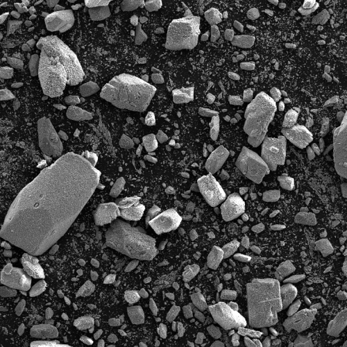
Real Material Differences: Morphology and Phase Characteristics
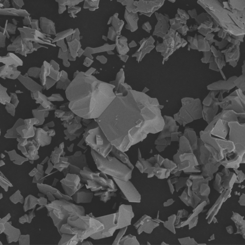
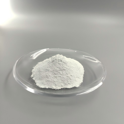
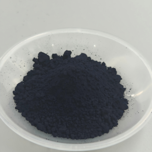
Material characterization clearly highlights the differences between MoO2 and MoO3 powders. MoO2 typically forms dense, compact particles with a darker appearance and higher packing density, reflecting its conductive monoclinic crystal structure. In contrast, MoO3 exhibits layered or plate-like particles, lighter coloration, anisotropic crystal growth, and lower packing density, consistent with the layered orthorhombic α-MoO3 structure. These morphological differences significantly affect industrial powder processing, influencing sintering behavior, evaporation stability, film uniformity, powder flowability, and electrode dispersion.
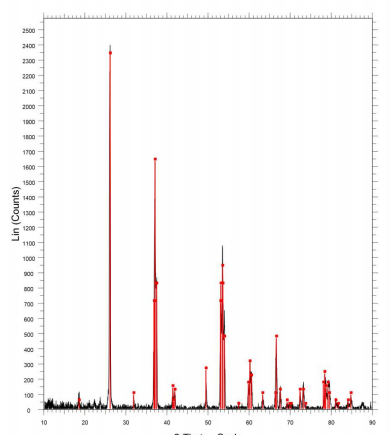
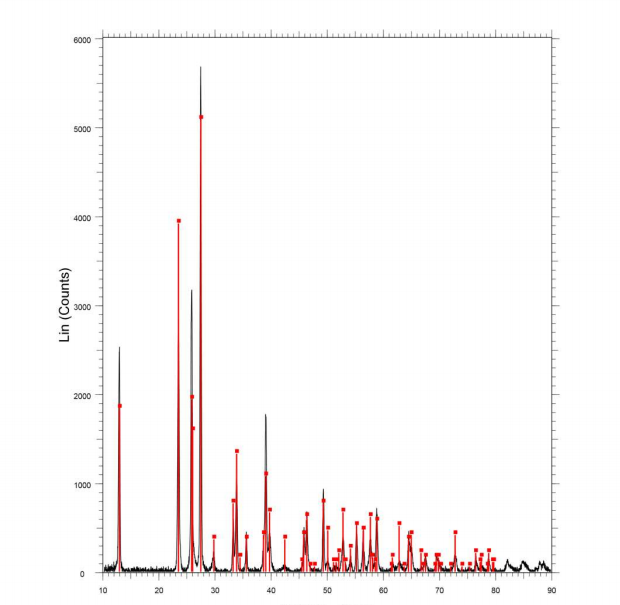
X-ray Diffraction (XRD) for MoOx Phase Identification
MoO2 XRD Features:
- Monoclinic diffraction peaks
- Rutile-like distortion signatures
- Broader reflections associated with conductive phase ordering
α-MoO3 XRD Features:
- Sharp orthorhombic diffraction peaks
- High crystallinity
- Layered phase reflections
Industrial Use of XRD:
- Confirm phase purity
- Monitor oxidation behavior
- Detect MoOx intermediate phases
- Evaluate thermal stability
- Ensure thin film process consistency
Notes for Vacuum Coating and Semiconductor Applications:
- Phase control is critical because electrical performance strongly depends on stoichiometry
MoO2 Properties: Why MoO2 Is a Conductive Oxide
MoO2 is widely recognized as a conductive transition metal oxide due to its partially filled Mo 4d orbitals, orbital overlap between adjacent Mo atoms, delocalized electronic states, and intrinsic conductivity. Unlike conventional semiconductors, which rely heavily on thermally activated carriers, MoO2 provides intrinsic electron transport, making it a highly efficient material for various advanced applications. Its metallic-like conductivity enables battery electrodes to achieve improved electron flow and reduces the need for carbon conductive additives in lithium-ion systems.
In hydrogen evolution reaction (HER) electrocatalysis, MoO₂ facilitates fast electron transfer, enhancing catalytic efficiency. The material’s properties also make it suitable for supercapacitors, where it lowers internal resistance, and for conductive coatings and thin film systems, providing stable electrical transport and good charge mobility.
Key applications and advantages include:
- Battery electrodes: improved conductivity, reduced carbon additive dependency
- HER electrocatalysis: fast electron transfer
- Supercapacitors: lower internal resistance
- Conductive coatings & thin films: stable transport and high charge mobility
MoO3 Properties: Why MoO3 Is Used in OLED and Thin Film Applications
Although MoO3 has relatively low intrinsic conductivity, its electronic structure and energy level characteristics make it extremely valuable in advanced electronics. The material features a wide band gap (~2.8–3.2 eV), high work function (~5.3–6.9 eV), strong electron-accepting ability, and excellent energy level alignment, which together enable efficient charge transport and interface performance in functional devices.
These properties make MoO3 a preferred material for OLED hole injection layers (HIL), organic semiconductor interfaces, vacuum thermal evaporation, transparent electronics, gas sensors, and electrochromic coatings.In OLED manufacturing, MoO₃ contributes to improved hole injection efficiency, enhanced interface stability, longer device lifetime, and better power efficiency. For this reason, high-purity MoO₃ evaporation materials are highly sought after in vacuum coating and thin film industries.
Key properties and applications include:
- Wide band gap (~2.8–3.2 eV): enables semiconducting behavior
- High work function (~5.3–6.9 eV): improves hole injection efficiency
- Strong electron-accepting ability & energy level alignment: enhances interface performance
- Applications: OLED HIL, organic semiconductor interfaces, vacuum thermal evaporation, transparent electronics, gas sensors, electrochromic coatings
- OLED benefits: improved hole injection, interface stability, device lifetime, and power efficiency
ULPMAT provides high-purity MoO₂ and MoO₃ powders, granules, and customized molybdenum oxide materials for thin film deposition, battery materials, and advanced electronic applications.
How Oxygen Vacancies Tune MoOx Properties
n real industrial materials, molybdenum oxides rarely exist as perfectly stoichiometric compounds. Most often, they form MoOx systems where some oxygen atoms are missing, creating oxygen vacancies. These vacancies play a critical role in tuning material properties. They can increase electrical conductivity, introduce defect states, modify optical absorption, change catalytic activity, and adjust the band structure.
As the concentration of oxygen vacancies increases, the material gradually transitions from MoO₃ → MoO₃₋ₓ → MoO₂-like behavior, creating a continuum between semiconducting and conductive states.
This tunability makes MoOx materials highly versatile and the focus of research for applications such as:
- Memristors and resistive switching devices
- Neuromorphic computing components
- Smart and functional coatings
- Gas sensing layers
Thermal Stability and Vacuum Processing of MoO2 and MoO3
MoO₂ and MoO₃ show distinctly different behaviors when exposed to heat and vacuum conditions. MoO₂ tends to oxidize into MoO₃ in oxygen-containing environments, typically around 400–500°C, so this oxidation must be carefully controlled during thermal processing to maintain its conductive properties.
In contrast, MoO₃ exhibits significant sublimation under vacuum, occurring around 650–700°C. This relatively high vapor pressure makes MoO₃ highly suitable for thermal evaporation, PVD coating, OLED deposition, and optical thin film manufacturing. Its controlled evaporation and high purity requirements are key reasons why MoO₃ is widely used in vacuum deposition systems and thin film applications.
Key points of thermal and vacuum behavior include:
- MoO₂: oxidizes to MoO₃ at ~400–500°C, requiring careful process control
- MoO₃: sublimes at ~650–700°C, making it ideal for thermal evaporation and PVD processes
- Applications influenced by thermal behavior: OLED deposition, optical thin films, vacuum coatings
Industrial Application Comparison
| Application Area | MoO2 | MoO3 |
| Conductive electrodes | Strong | Weak |
| OLED devices | Limited | Strong |
| Battery systems | Strong | Moderate |
| Electrocatalysis | Strong | Moderate |
| Gas sensors | Moderate | Strong |
| Vacuum evaporation | Limited | Strong |
| Conductive thin films | Strong | Moderate |
| Electrochromic devices | Moderate | Strong |
How to Choose the Right MoOx Material?
Selecting the appropriate molybdenum oxide material depends on the specific requirements of your application. MoO₂ is ideal for applications that demand high conductivity, such as conductive ceramics, battery electrodes, electrocatalysis, conductive thin films, and systems requiring low electrical resistance. On the other hand, MoO₃ is better suited for semiconducting or interface-focused applications, including OLED layers, vacuum evaporation materials, optical thin films, and gas sensing devices.
For advanced applications, oxygen-deficient MoOx materials offer a tunable balance between conductivity and semiconducting behavior, providing flexibility for customized electronic and energy solutions.
Key considerations:
- MoO2: conductive ceramics, battery electrodes, electrocatalysis, conductive thin films, low resistance
- MoO3: OLED interfaces, vacuum evaporation, optical thin films, gas sensors
- MoOx (oxygen-deficient): adjustable properties for mixed conductivity and semiconducting applications
High-Purity MoO2 and MoO3 for Industrial Applications
High-purity MoO2 and MoO3 are essential for industrial applications where performance and consistency are critical. These materials are widely used in semiconductor manufacturing, OLED deposition, vacuum coating, advanced batteries, research laboratories, and thin film R&D.
When sourcing MoOx materials, key specifications to consider include purity level, particle size distribution, oxygen stoichiometry, phase composition, evaporation stability, tap density, and impurity control. Ensuring consistent material quality is particularly important for vacuum deposition and electronic applications.
For industrial evaluation, it is recommended to request detailed technical documentation, such as:
- COA (Certificate of Analysis)
- TDS (Technical Data Sheet)
- SEM/XRD characterization
- Purity analysis and particle size data
These documents help verify that the MoOx material meets your process and application requirements, ensuring reliable performance in high-precision industrial systems.For applications requiring molybdenum trioxide materials, ULPMAT provides high-purity MoO3 Powder with controlled purity and particle characteristics.
Conclusion
The fundamental difference between MoO2 and MoO3 arises from their oxidation states, crystal structures, and electron distribution. MoO₂ exhibits conductive behavior due to partially filled Mo 4d orbitals and a dense monoclinic lattice that allow efficient electron delocalization, while MoO₃ behaves as a semiconductor because fully oxidized Mo⁶⁺ ions form a wide band gap (~2.8–3.2 eV) and a layered orthorhombic structure that limits charge transport. Between these extremes lies the broader MoOx system, where oxygen vacancy engineering enables continuous tuning of electrical and optical properties for advanced electronic and energy applications. As demand for high-performance thin films, electronic ceramics, and vacuum-coated materials grows, both MoO₂ and MoO₃ remain key strategic materials in semiconductor, energy, and vacuum coating industries.
FAQ
Q1: What is the difference between MoO₂ and MoO₃?
A1:MoO₂ and MoO₃ are two important molybdenum oxide materials with different oxidation states and electronic properties. MoO₂ contains Mo⁴⁺ and exhibits metallic-like conductivity, while MoO₃ contains Mo⁶⁺ and behaves as a semiconductor with a wide band gap. These differences determine their applications in batteries, thin films, OLED devices, and vacuum deposition.
Q2: Why is MoO₂ electrically conductive?
A2:MoO₂ shows conductive behavior because its partially filled Mo 4d orbitals allow electron transport through Mo–Mo bonding networks. This metallic-like conductivity makes MoO₂ suitable for conductive coatings, battery electrodes, electrocatalysis, and electronic materials.
Q3: Why is MoO₃ used in OLED and thin film applications?
A3:MoO₃ is widely used in OLED and thin film applications because of its high work function, electron-accepting ability, and suitable energy level alignment. These properties improve charge injection and interface performance in electronic devices.
Q4: What purity of molybdenum oxide is required for electronic applications?
A4:High-purity molybdenum oxide materials are typically required for electronic, OLED, and thin film applications. Purity, phase composition, particle size, and impurity control are important factors affecting deposition performance and final device properties.
Q5: Can MoO₂ and MoO₃ be used interchangeably?
A5:No. MoO₂ and MoO₃ have different electrical properties, crystal structures, and application requirements. MoO₂ is preferred for conductive applications, while MoO₃ is commonly selected for semiconductor, OLED, evaporation, and optical thin film applications.
Q6: What forms of molybdenum oxide materials are available?
A6:Molybdenum oxide materials are available in different forms including powders, granules, and targets. The appropriate form depends on the application, such as powder synthesis, vacuum evaporation, sputtering, ceramic processing, or thin film deposition.