What is boron nitride? How is it classified?
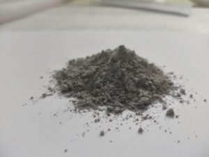
Boron nitride (BN) is an advanced ceramic material composed of boron and nitrogen atoms arranged in a layered crystal structure, similar to graphite. It is highly valued in semiconductor manufacturing due to its combination of thermal stability, electrical insulation, and chemical inertness. BN is typically available in powder form for processing into hot-pressed ceramics, coatings, and insulating components used in CVD, PVD, plasma etching, and wafer handling equipment.
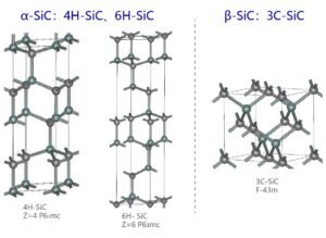
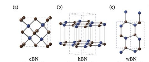
Boron nitride is classified into three main crystal structures:
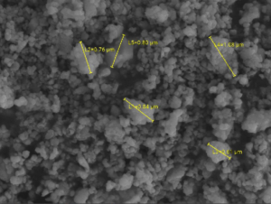
- Hexagonal BN (h-BN): The most common form in semiconductor applications, offering excellent thermal and electrical properties with machinability.
- Cubic BN (c-BN): Extremely hard, used in cutting tools and abrasive applications, less common in semiconductor equipment.
- Wurtzite BN (w-BN): Rare and highly specialized, mainly used in high-pressure research and extreme engineering applications.
Within each type, BN materials are further categorized by purity, particle size, density, and processing method, which determine their suitability for specific high-temperature, plasma-resistant, or ultra-clean semiconductor applications.
Why Hexagonal Boron Nitride Is Used in Semiconductor Equipment?
Hexagonal boron nitride in semiconductor applications is widely used because it combines excellent thermal stability, electrical insulation, and resistance to plasma attack. Semiconductor manufacturing processes such as CVD, PVD, and plasma etching expose materials to extreme conditions including temperatures from 800°C to 1800°C, high-energy plasma, and ultra-high vacuum environments.
h-BN ceramic materials maintain structural integrity and dielectric stability under these conditions, making them one of the most reliable thermal insulation ceramics in advanced semiconductor equipment.
High Temperature Stability of h-BN Ceramic Materials
Hexagonal boron nitride (h-BN) exhibits excellent high-temperature stability. In inert or vacuum environments, its operating temperature can reach approximately 1800°C. In oxidizing atmospheres, its actual operating temperature is approximately 850–900°C, making h-BN suitable for furnace insulation systems, wafer carriers, and high-temperature structural components. Its extremely low coefficient of thermal expansion (approximately 1–2 × 10⁻⁶ /K) reduces thermal stress and improves the long-term operational stability of semiconductor devices.
Thermal and electrical properties of hexagonal boron nitride
The performance of hexagonal boron nitride in semiconductor applications is mainly driven by its unique combination of thermal conductivity and electrical insulation. Typical properties include thermal conductivity ranging from 15 to 96 W/m·K, electrical resistivity of 10¹³–10¹⁵ Ω·cm, and dielectric strength up to 200 kV/mm depending on density and structure.
These properties allow h-BN ceramic materials to dissipate heat efficiently while maintaining excellent electrical isolation in RF plasma environments.
| Property | Typical Value |
| Thermal conductivity | 15–96 W/m·K |
| Electrical resistivity | 10¹³–10¹⁵ Ω·cm |
| Dielectric strength | 50–200 kV/mm |
How BN Ceramics Resist Plasma in Semiconductor Manufacturing
Plasma processes in semiconductor manufacturing generate highly reactive species such as fluorine, chlorine, and oxygen radicals. Hexagonal boron nitride demonstrates strong resistance to plasma attack due to its stable covalent bonding and chemical inertness.
As a result, h-BN ceramic materials are widely used in plasma-facing components such as chamber liners, insulating supports, and shielding parts. Compared with alumina (Al2O3) and silica (SiO2), BN materials show lower particle generation and significantly improved surface durability, which helps maintain wafer yield and process stability.
Electrical Insulation Properties of Hexagonal Boron Nitride
In RF-driven semiconductor systems, dielectric stability is essential for plasma control. Hexagonal boron nitride provides stable dielectric constant (~4.0–4.4), high resistivity, and consistent breakdown strength.These properties ensure stable plasma distribution, reduced electrical interference, and improved precision in semiconductor processing systems.
Contamination Resistance and Machinability of Boron Nitride
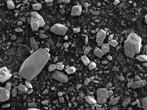
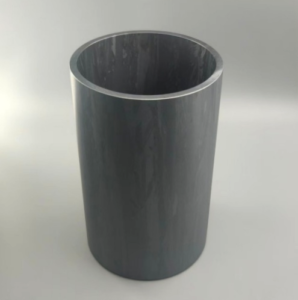
For advanced semiconductor nodes, contamination control is critical at ppm and ppb levels. Hexagonal boron nitride in semiconductor applications is preferred because it contains no mobile metallic ions, shows extremely low outgassing under vacuum (<10⁻⁹ Torr), and remains chemically inert in most process gases.Hot-pressed h-BN ceramics derived from powder can be machined into complex shapes using conventional tools, enabling flexible design of wafer fixtures, spacers, and furnace components.
Applications of h-BN in Semiconductor Equipment
Hexagonal boron nitride is widely used in semiconductor manufacturing equipment depending on purity, density, and plasma exposure requirements.
| Equipment Type | Application |
|---|---|
|
CVD systems |
Thermal insulation and hot-zone components |
|
PVD systems |
Thermal shielding and supports |
|
Plasma etching |
Chamber liners and insulating rings |
|
Thermal furnaces |
High-temperature insulation parts |
|
Precision ceramic components |
Wafer handling |
Importance of h-BN for Advanced Semiconductor Nodes
As semiconductor nodes shrink to 5nm and below, process environments become more sensitive to contamination, thermal drift, and plasma instability. Hexagonal boron nitride in semiconductor applications provides long-term thermal stability, strong plasma resistance, stable dielectric behavior, and ultra-low contamination risk.
These properties make h-BN ceramic materials a critical enabling material for next-generation semiconductor manufacturing systems.
Conclusion
Hexagonal boron nitride is one of the most reliable plasma resistant ceramic materials for semiconductor equipment. Its combination of high thermal stability (up to ~1800°C), thermal conductivity (15–96 W/m·K), high electrical resistivity (10¹³–10¹⁵ Ω·cm), chemical inertness, and machinability makes it essential for high-temperature, plasma-rich, and ultra-clean semiconductor environments.