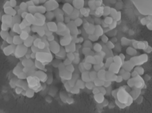

Crystalline silicon (c-Si) is an elemental semiconductor widely used in solar cells, semiconductor devices, and advanced materials research. Its properties depend on crystal structure, chemical purity, defects, and processing conditions. Understanding the differences between monocrystalline, polycrystalline, and amorphous silicon helps researchers and engineers select the appropriate material for a specific application.
For industrial and laboratory processes, crystal structure is only one part of material selection. Purity, physical form, particle size, surface condition, and processing requirements can also determine whether a silicon material is suitable. This guide explains the key properties of crystalline silicon, compares its major forms, and outlines the factors to evaluate when sourcing silicon materials from suppliers such as ULPMAT.
What Is Crystalline Silicon?
Crystalline silicon is elemental silicon (Si) in which atoms are arranged in a regular, repeating three-dimensional crystal lattice. This long-range atomic order gives crystalline silicon its characteristic semiconductor behavior and optical properties. Silicon has a diamond-cubic crystal structure under normal ambient conditions. Its electronic properties make it fundamental to conventional photovoltaic cells, integrated circuits, and many other semiconductor technologies.
Crystalline silicon is not a single product specification. It can refer to different crystal forms and materials supplied as wafers, ingots, pieces, granules, or powders. These descriptions represent different characteristics:
Crystal structure: How silicon atoms are arranged within the material.
Chemical purity: The proportion of silicon and the concentration of impurities.
Physical form: Whether the material is supplied as a wafer, piece, granule, or powder.
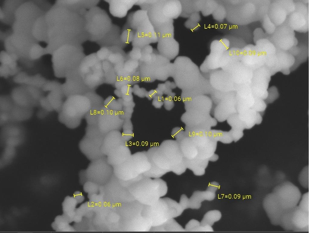
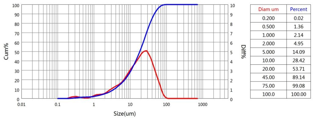
Particle size: The dimensions and distribution of particles in particulate materials.
Surface condition: The presence of oxide layers, contamination, or other surface features.
These characteristics should be evaluated separately. For example, high chemical purity does not automatically establish that a material is monocrystalline, and a crystalline silicon powder is not equivalent to a semiconductor-grade silicon wafer.
Key Properties of Crystalline Silicon
The following properties explain why crystalline silicon is widely used in electronics, photovoltaics, and materials research.
| Property | Description | Relevance to material selection |
| Chemical symbol | Si | Identifies elemental silicon |
| Crystal structure | Diamond cubic | Defines its ordered atomic arrangement |
| Room-temperature band gap | Approximately 1.12 eV | Relevant to semiconductor and photovoltaic behavior |
| Density | Approximately 2.33 g/cm³ for crystalline silicon | Useful for material calculations and processing |
| Melting point | Approximately 1,414°C | Relevant to high-temperature processing |
| Electrical behavior | Semiconductor | Can be modified through doping and device processing |
These values are typical reference values for crystalline silicon.
1. Crystal Structure and Defects
The ordered crystal lattice distinguishes crystalline silicon from amorphous silicon. However, crystalline materials can still contain vacancies, dislocations, grain boundaries, and impurities. In semiconductor applications, these defects can influence carrier transport, recombination, and device performance. The significance of each defect depends on the intended application and manufacturing process.
For industrial feedstocks and laboratory experiments, the required level of crystal quality should be determined by the process rather than assumed from the material name.
2. Semiconductor Properties
Silicon has electrical properties between those of conductors and insulators. Its electrical behavior can be modified through doping, junction formation, and other processing steps. For semiconductor wafers, important parameters may include resistivity, dopant concentration, crystal orientation, and defect density. For silicon used in chemical synthesis or general materials research, chemical purity, particle size, and surface condition may be more important.
3. Optical Properties
Crystalline silicon interacts with light in ways that make it useful in photovoltaic devices and optical research. Its optical response depends on wavelength, thickness, surface condition, and material quality. In solar cells, silicon absorbs photons and generates charge carriers. The final conversion efficiency also depends on cell architecture, surface passivation, electrical contacts, and manufacturing conditions.
4. Thermal and Chemical Behavior
Silicon has a high melting point and is used in processes involving elevated temperatures. Its surface can oxidize when exposed to oxygen, and its behavior during heating, etching, or chemical reactions depends on the process environment. Temperature, atmosphere, surface oxide, and contact with other materials can affect processing outcomes. These factors should be considered when selecting silicon for synthesis, coating, or other industrial applications.
Monocrystalline Silicon vs. Polycrystalline Silicon
Monocrystalline silicon and polycrystalline silicon are both crystalline forms of elemental silicon. Their principal difference is the number and arrangement of crystal grains.
| Characteristic | Monocrystalline Silicon | Polycrystalline Silicon |
| Crystal structure | One continuous crystal lattice | Multiple crystalline grains |
| Grain boundaries | No boundaries between separate grains within the single crystal | Boundaries occur between grains |
| Crystal orientation | Continuous across the crystal | Varies between grains |
| Typical applications | Semiconductor wafers and many high-performance solar cells | Selected photovoltaic, semiconductor, and industrial processes |
| Important quality factors | Crystal defects, orientation, resistivity, and impurities | Grain structure, defects, purity, and process requirements |
Monocrystalline silicon is widely used in semiconductor manufacturing because its continuous crystal structure supports precise device fabrication. Polycrystalline silicon also has important industrial applications, with suitability determined by the required material properties and manufacturing method.
Neither form is automatically the best choice for every application. Cost, crystal quality, processing requirements, and final performance all influence material selection.
Crystalline Silicon vs. Amorphous Silicon
Crystalline silicon and amorphous silicon have the same elemental composition but different atomic arrangements. Crystalline silicon has long-range periodic order, whereas amorphous silicon lacks long-range periodic order.
| Comparison | Crystalline Silicon | Amorphous Silicon |
| Atomic arrangement | Long-range periodic order | Disordered atomic network |
| Common photovoltaic form | Wafer-based silicon cells | Thin-film silicon cells |
| Typical processing | Crystal growth, wafer preparation, and device fabrication | Thin-film deposition, often using plasma-enhanced chemical vapor deposition |
| Key considerations | Crystal quality, defects, and electrical properties | Film composition, thickness, defect passivation, and deposition conditions |
Crystalline silicon is the principal material used in conventional wafer-based solar cells. Hydrogenated amorphous silicon (a-Si) is used in selected thin-film photovoltaic and electronic applications.The choice depends on the device architecture and manufacturing process. Crystalline silicon is suited to applications requiring an ordered crystal structure, while amorphous silicon can be useful in thin-film technologies.
It is also important not to confuse amorphous silicon (Si) with amorphous silica (SiO₂). Amorphous silicon is an elemental form of silicon, whereas silica is a silicon-oxygen compound with different chemical properties and applications.
Applications of Crystalline Silicon
Solar Cells and Photovoltaics:Crystalline silicon is widely used in conventional photovoltaic manufacturing. Silicon is processed into wafers, which are then fabricated into solar cells and assembled into modules.Monocrystalline silicon is common in modern solar modules. Wafer quality, cell architecture, surface treatment, and manufacturing conditions all contribute to the performance of the finished device.
Semiconductors and Microelectronics:High-purity crystalline silicon is a fundamental substrate material for integrated circuits and many semiconductor devices. Controlled impurity concentrations, crystal defects, and electrical properties are essential for reliable device fabrication.Silicon intended for semiconductor wafer production should not automatically be treated as interchangeable with general-purpose silicon feedstock. The physical form, purity, and electrical specifications must match the intended manufacturing stage.
Materials Research and Laboratory Processes:Silicon is used in research involving semiconductor processing, surface reactions, material synthesis, and the development of silicon-containing compounds.Different experiments may require different physical forms. Semiconductor studies may require wafers or single-crystal substrates, whereas chemical reactions and synthesis processes may require pieces, granules, or powder.For particulate starting materials, purity, particle-size distribution, and surface condition may be more relevant than wafer orientation or electrical resistivity.
Silicon-Based Material Synthesis:Elemental silicon can serve as a starting material in selected synthesis and reaction processes. Depending on the reaction mechanism, researchers may need to control particle size, morphology, impurity content, or surface oxide.The appropriate specification should be based on the intended reaction and downstream process. A general product name alone cannot establish suitability.
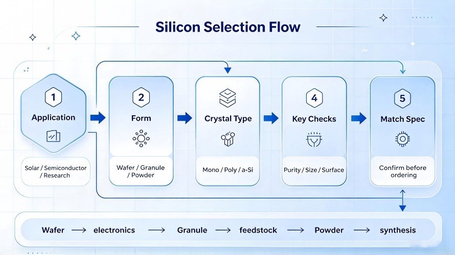
How to Select Silicon for Industrial Applications
Start with the intended application, then check which material properties matter most.
Step 1 — Identify the Required Form
Wafer or substrate → Check crystal orientation, resistivity, and defects.
Pieces or granules → Check dimensions, purity, and feeding requirements.
Powder → Check purity, particle size, distribution, and surface condition.
Step 2 — Confirm Purity Requirements
Does the process have strict impurity limits?
→ Yes: Identify critical elements and verify analytical data.
→ No: Confirm the stated purity and test method.
Step 3 — Check Particle Size and Surface Condition
For powders and granules, confirm the particle-size range and measurement method. If surface reactions are important, consider oxidation, storage, and contamination.
Step 4 — Match the Specification to the Application
Semiconductor substrates → Prioritize electrical and crystal properties.
Chemical synthesis → Prioritize purity, critical impurities, and surface condition.
Powder processing → Prioritize particle size, distribution, and handling behavior.
Step 5 — Confirm Before Ordering
Check the material form, purity, critical impurity limits, dimensions or particle size, packaging, and available documentation.
ULPMAT provides silicon material options for research and industrial applications. Review the silicon granules specifications and confirm suitability before ordering. For processes requiring powder, select a compatible powder grade rather than assuming granules are interchangeable.
FAQs
1. What is crystalline silicon mainly used for?
Its main applications are solar cells, semiconductor devices, and microelectronics. It is also used in materials research and selected industrial processes where silicon composition, crystal structure, or physical form affects the result.
2. How does monocrystalline silicon differ from polycrystalline silicon?
Monocrystalline silicon has a continuous crystal lattice, while polycrystalline silicon consists of multiple crystal grains separated by grain boundaries. These boundaries can influence electrical transport and other material properties. The better choice depends on the required performance and manufacturing process.
3. How does crystalline silicon differ from amorphous silicon?
The key difference is atomic order. Crystalline silicon has a regular, long-range atomic arrangement, whereas amorphous silicon lacks long-range periodic order. This affects electronic behavior and processing methods, including the distinction between wafer-based devices and thin-film applications.
4. Is silicon powder necessarily crystalline?
No. Powder describes particle form, not atomic structure. A powder can contain crystalline silicon, but particle size alone cannot establish crystallinity. When crystal structure matters, check whether suitable characterization data, such as X-ray diffraction results, are available.
5. Does higher silicon purity guarantee better performance?
No. Purity indicates the level of chemical contamination, but it does not establish crystal quality, particle-size distribution, surface condition, or suitability for a particular process. The relevant impurity limits depend on the application; electrically active contaminants can be especially important in semiconductor materials.
6. How do I choose the right particle size for silicon powder?
Start with the process requirements. Particle size can affect surface area, flow, packing, dispersion, and reaction behavior. Confirm the required size range, distribution, and measurement method, because sieve analysis and laser diffraction do not necessarily produce directly comparable results.
7. What information should I request before purchasing silicon for research or production?
Confirm the chemical composition, stated purity and its measurement basis, physical form, particle-size specifications where applicable, critical impurity limits, packaging, and available analytical documentation. If the process depends on crystallinity or surface condition, request evidence for those properties separately rather than inferring them from the product name.
8. Where can I check silicon material specifications from ULPMAT?
ULPMAT provides silicon material options for research and industrial applications. The ULPMAT silicon granules product page lists information for that product form. Check the published specifications against your process requirements, and confirm any unlisted parameters with ULPMAT before ordering. If your process requires powder, verify the specifications of a suitable powder grade separately.
Conclusion
Silicon selection depends on more than purity alone. Crystal structure, impurity levels, physical form, particle size, and surface condition all influence whether a grade is suitable for a particular application.
For research and industrial use, start with the process requirements and verify the specifications that directly affect performance. ULPMAT provides silicon material options for different applications, allowing buyers to compare available grades and confirm suitability before ordering.
Explore ULPMAT’s silicon material specifications to compare available grades and identify a suitable option for your application.
References
- 1. U.S. Department of Energy. Crystalline Silicon Photovoltaics Research.
- 2. U.S. Department of Energy. PV Cells 101: A Primer on the Solar Photovoltaic Cell.
- 3. U.S. Department of Energy. Solar Photovoltaic Cell Basics.
- 4. Ballif, C., et al. “Status and Perspectives of Crystalline Silicon Photovoltaics in Research and Industry.” Nature Reviews Materials, 2022.