Overview of Sputtering Targets in Modern Electronics
Sputtering targets are essential materials used in Physical Vapor Deposition (PVD) processes to create thin films on various substrates. These thin films are widely applied in semiconductors,optoelectronics, energy devices, and advanced coatings.As demand for high-performance materials continues to grow, high purity sputtering targets have become critical for ensuring film quality, consistency, and device reliability.
What is a Sputtering Target?
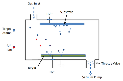
A sputtering target is a solid material used as the source in sputtering deposition, a widely used thin-film fabrication technique in electronics, optics, and materials science. During the sputtering process, energetic ions—usually from a plasma—strike the target surface, knocking off atoms or clusters of atoms. These ejected particles travel through the vacuum and deposit onto a substrate, gradually forming a uniform thin film with controlled thickness and composition.
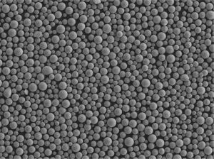
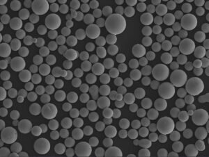
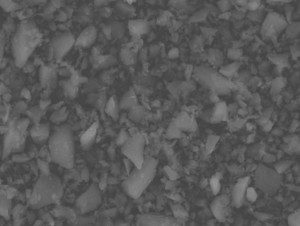
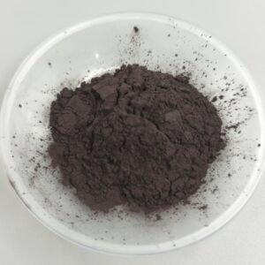
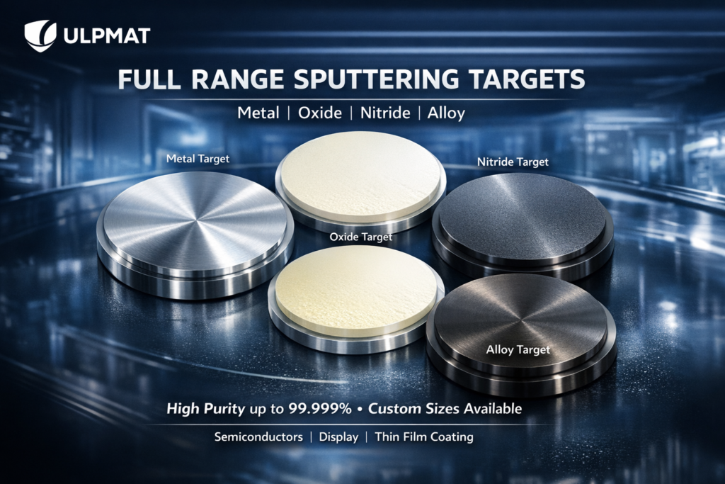
Sputtering targets can be made from metals, alloys, oxides, nitrides, or other compounds, depending on the desired film properties. The choice of target material directly influences the film’s adhesion, conductivity, optical characteristics, and chemical stability. High-purity targets are essential for achieving consistent thin-film quality, especially in semiconductor, photovoltaic, and optical coating applications.
Types of Sputtering Target Materials
Sputtering targets are essential components in thin film deposition processes. They serve as the source material that is bombarded by energetic ions, releasing atoms that form uniform thin films on substrates. The choice of target material directly affects the properties and performance of the resulting film. Targets are generally classified based on their composition and functional properties:
Metal Targets
Metal sputtering targets are widely used due to their excellent electrical and thermal conductivity. Common examples include aluminum (Al), copper (Cu), nickel (Ni), titanium (Ti), and gold (Au). These metals are primarily used in applications where conductive layers or interconnects are required.
Ceramic Targets
Ceramic targets consist of inorganic, non-metallic compounds that provide specialized optical, electrical, or mechanical properties. Examples include indium tin oxide (ITO), zinc oxide (ZnO), titanium dioxide (TiO₂), and vanadium oxide (VO₂). Ceramic targets are often used when transparency, resistivity control, or specific functional responses are required.
Alloy Targets
Alloy sputtering targets are composed of two or more metallic elements, or metals combined with ceramics, to achieve enhanced or tailored properties. Examples include NiCr, CuSn, TiAl, and CoFeB. Alloy targets are used to optimize conductivity, thermal resistance, magnetic properties, or mechanical strength in the thin film.
Key Applications of Sputtering Targets
Sputtering targets are critical in producing high-performance thin films for a wide range of industrial applications. Their versatility allows them to meet the needs of advanced electronics, energy systems, and smart material technologies.
Semiconductor Manufacturing
Metal, alloy, and some ceramic targets are extensively used in semiconductor fabrication. Sputtering is a key process for depositing conductive, barrier, and dielectric layers in integrated circuits and microelectronic devices.
Optoelectronics
Sputtering targets play a crucial role in optoelectronic devices, enabling thin films with tailored optical and electrical properties. Ceramics like ITO or oxides like ZnO are widely used to create transparent conductive layers.
Energy Devices
Sputtering targets are also essential in the energy sector, particularly in thin-film energy storage and conversion systems. Metal, alloy, and ceramic targets contribute to efficient energy devices.
Smart Materials
Advanced oxide and ceramic targets enable functional coatings for smart materials. For example, VO₂ sputtering targets are used to create thermochromic thin films that respond to temperature changes.
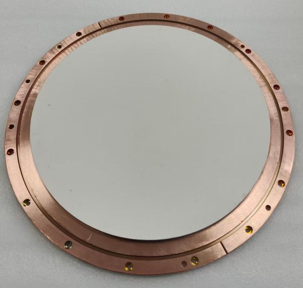
Custom Sputtering Targets and Manufacturing Capabilities
In advanced applications, standard targets may not meet specific requirements. Custom sputtering targets allow optimization in:
- Material composition
- Dimensions and shapes
- Bonding with backing plates
Reliable suppliers provide consistent quality, precise machining, and stable delivery.
Conclusion
Sputtering targets are fundamental materials in modern thin-film technology. Their role spans across semiconductors, energy, and advanced functional coatings.
Selecting high purity sputtering targets and a reliable supplier is essential for achieving consistent performance and long-term stability.