

Perovskite sputtering targets are special multi‑element PVD materials used to produce various perovskite thin‑films for photovoltaics, optoelectronics, semiconductors and materials research. They come in a wide range of compositions with typical representative formulas, and proper considerations are critical when selecting or customizing these targets.
What Is Perovskite Sputtering Target?
Perovskite sputtering targets are solid perovskite-based materials used in physical vapor deposition (PVD), particularly magnetron sputtering, to deposit functional perovskite thin films. Perovskites are a class of materials with a characteristic crystal structure, commonly represented by ABX₃. In halide perovskites, A can include Cs⁺, methylammonium (MA⁺), or formamidinium (FA⁺), B is commonly Pb²⁺ or Sn²⁺, and X is typically Cl⁻, Br⁻, or I⁻.
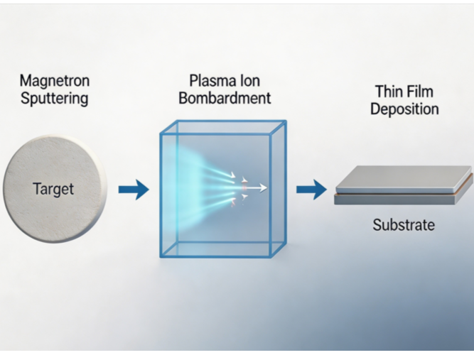
During sputtering, plasma ions bombard the target surface and eject material toward the substrate, where it forms a thin film. Target composition, purity, and sputtering conditions can affect the composition and properties of the deposited film. Perovskite sputtering targets therefore cover a range of compositions and structures for thin-film research and development in photovoltaic, optoelectronic, and semiconductor applications.
Types of Perovskite Sputtering Targets
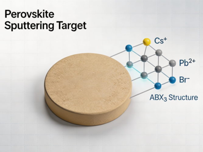
Perovskite sputtering targets can be classified according to their chemical composition and crystal structure. The main categories include cesium-based perovskites, doped and composition-engineered perovskites, lead-free perovskites, and double perovskites.
| Perovskite Type | Typical Examples | Main Characteristics |
| Cesium-based perovskites | CsPbBr₃, CsPbCl₃, CsPbI₃ | Inorganic halide perovskites with tunable halide composition |
| Doped and composition-engineered perovskites | CsPb₁₋ₓZnₓBr₃, Mn-doped CsPbBr₃ | Modified composition for tailored material properties |
| Lead-free perovskites | CsSnBr₃, CsSnI₃, Bi-based, Sb-based systems | Alternative B-site chemistry without Pb |
| Double perovskites | Cs₂AgBiBr₆, Cs₂AgBiCl₆, Cs₂AgInCl₆ | Cs₂AgBiBr₆, Cs₂AgBiCl₆, Cs₂AgInCl₆ |
- Cesium-Based Perovskite Sputtering Targets
- Doped and Composition-Engineered Perovskite Targets
- Lead-Free Perovskite Sputtering Targets
- Double Perovskite Sputtering Targets
Perovskite Target Materials and Key Properties
The performance of a perovskite sputtering target depends not only on its chemical formula but also on factors such as composition accuracy, purity, density, microstructure, mechanical strength, and compatibility with the sputtering process.
1. Perovskite Crystal Chemistry
Many halide perovskites are based on the general ABX₃ crystal structure, where:
A = monovalent cation, such as Cs⁺, MA⁺, or FA⁺
B = metal cation, such as Pb²⁺ or Sn²⁺
X = halide anion, such as Cl⁻, Br⁻, or I⁻
The substitution of A-site, B-site, or X-site components can modify the structural, optical, and electronic properties of perovskite materials. For example, changing the halide composition from Cl to Br or I can influence optical absorption and emission characteristics, while B-site substitution can affect material stability and electronic behavior.This flexibility allows perovskite sputtering targets to be prepared with a wide range of compositions for different thin-film applications.
2. Chemical Composition
Accurate chemical composition is essential for multi-element perovskite sputtering targets. Key factors include elemental ratio, halide ratio, dopant concentration, phase composition, and stoichiometric control.For materials such as CsPb₀.₅Zn₀.₅Br₃, the relative proportions of Cs, Pb, Zn, and Br need to be precisely controlled to achieve the required target composition.
3. Purity
Target purity is an important consideration for photovoltaic, optoelectronic, and semiconductor-related applications. Impurities may influence film composition, defect concentration, optical properties, electrical performance, and process reproducibility.The required purity level depends on the specific application and deposition requirements.
4. Density and Microstructure
Target density and microstructure can affect sputtering stability and target utilization. Important characteristics include bulk density, porosity, grain structure, mechanical strength, and surface condition.A well-prepared target with suitable density and mechanical integrity can support stable sputtering performance and reduce particle-related issues during deposition.
5. Thermal and Chemical Stability
The thermal and chemical stability of perovskite targets varies depending on their composition and structure. Factors such as chemical composition, crystal structure, dopant type, manufacturing process, storage conditions, and sputtering parameters can influence material stability.For certain perovskite systems, thermal exposure and plasma conditions may affect composition or phase structure. Therefore, target selection should consider both material characteristics and deposition conditions.
Perovskite Sputtering Target and Thin-Film Deposition Process
Perovskite thin-film deposition using sputtering involves a series of steps, starting from target selection and ending with film optimization. The target composition provides the material source, while sputtering conditions and post-deposition processes influence the final film structure and properties.
Perovskite Sputtering Target → Vacuum Chamber Preparation → Plasma Generation and Ion Bombardment → Sputtered Material Transfer → Thin-Film Deposition on Substrate → Post-Deposition Treatment and Film Optimization
The process begins with selecting a suitable perovskite sputtering target based on the required composition, purity, dimensions, and application requirements. For multi-element perovskites, the ratios of A-site, B-site, and halide components need to be carefully controlled to achieve the desired film composition. For example, CsPbBr₃ and CsPb₀.₅Zn₀.₅Br₃ contain different elemental compositions and may result in different thin-film characteristics.
During magnetron sputtering, the target is placed inside a vacuum chamber under a controlled atmosphere. Plasma-generated ions bombard the target surface and release material from the target. These sputtered species travel through the plasma and deposit onto the substrate, forming a perovskite thin film.
The quality of the deposited film depends on both target properties and process conditions, including sputtering power, working pressure, substrate temperature, deposition rate, film thickness, and post-deposition treatment. Thermal treatment or controlled crystallization may further influence phase formation, surface morphology, and film performance.Because different perovskite compositions have different structural and chemical characteristics, deposition conditions need to be adjusted according to the selected target material and intended application.
Applications of Perovskite Sputtering Targets
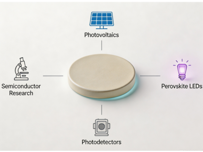
Perovskite sputtering targets are mainly used for the development of functional thin films in photovoltaic, optoelectronic, and semiconductor-related research. The application fields depend on the composition and properties of the selected perovskite material.
Perovskite Solar Cells:Perovskite materials are widely studied in photovoltaic research due to their adjustable optical properties and strong light absorption characteristics. Sputtering targets provide a vacuum deposition approach for preparing perovskite-related thin films and studying film composition, interfaces, and device structures.
Perovskite LEDs:Halide perovskites have attracted interest for light-emitting applications because their composition can influence optical emission properties. Perovskite sputtering targets can be used in thin-film research for exploring luminescent layers and optoelectronic device structures.
Photodetectors:Perovskite materials are investigated for photodetection applications due to their interaction with light and tunable electronic properties. Sputtered perovskite films can be evaluated for applications such as visible-light detection, optical sensing, and related optoelectronic devices.
Optical and Electronic Thin Films:Different perovskite compositions can provide different optical and electronic characteristics, making them suitable for thin-film studies involving light absorption, charge transport, and interface engineering.
Semiconductor and Materials Research:Perovskite sputtering targets are also used in laboratory research focused on thin-film growth, composition optimization, and deposition process development. Customized target compositions allow researchers to explore specific perovskite systems and material properties.
How to Select Perovskite Sputtering Target?
Selecting a perovskite sputtering target involves several steps, from defining the required material composition to confirming target specifications and sputtering compatibility. For multi-element perovskite materials, a clear selection process helps ensure that the target meets the requirements of the intended thin-film application.
Step 1: Define the Required Perovskite Composition
The first step is to determine the exact perovskite material system required for the application. Common compositions include CsPbBr₃, CsPbCl₃, CsPbI₃, CsPb₁₋ₓZnₓBr₃, and Cs₂AgBiBr₆.For customized perovskite sputtering targets, the chemical formula, elemental ratio, and dopant concentration should be clearly specified. This is especially important for doped or composition-engineered materials, where changes in element ratio may influence the structure and properties of the deposited film.
Step 2: Confirm Target Specifications
After defining the material composition, the target specifications should be matched with the sputtering equipment. The required information includes target shape, dimensions, thickness, mounting configuration, and whether a bonded or unbonded target is needed.For laboratory and industrial sputtering systems, the target geometry must be compatible with the cathode design to ensure proper installation and stable operation.
Step 3: Check Sputtering System Compatibility
The sputtering method and equipment configuration are important factors in target selection. Users should confirm whether the system uses RF or magnetron sputtering, as well as the target holder type and operating requirements.For complex perovskite materials, compatibility between the target and deposition system helps maintain stable sputtering performance and consistent film preparation.
Step 4: Match the Target with the Thin-Film Application
The final selection should be based on the intended thin-film application. Different research areas, including photovoltaic devices, optoelectronic components, and material development, may require different perovskite compositions and target designs.Providing information about the expected film composition, deposition purpose, and application requirements allows the target specification to be better aligned with the final objective.
Custom Perovskite Sputtering Targets
Custom Perovskite Sputtering Targets
Perovskite materials offer a wide range of compositional possibilities, making customized sputtering targets valuable for thin-film research and advanced material development. A custom perovskite sputtering target can be prepared according to the required composition, purity, dimensions, and sputtering system requirements.
Customized Material Composition
The chemical composition is the most important part of a customized perovskite sputtering target. Custom solutions can include cesium-based perovskites, doped perovskites, lead-free systems, mixed-halide compositions, and double perovskites.For composition-engineered materials, customers can provide either the complete chemical formula or the required elemental ratio. For example, CsPb₁₋ₓZnₓBr₃ can be customized according to the required Zn/Pb substitution ratio.
Customized Target Specifications
Perovskite sputtering targets can be manufactured in different sizes and configurations according to the requirements of the deposition system. Target diameter, length, width, thickness, geometry, and mounting configuration can be adjusted to match laboratory or industrial sputtering equipment.For specific systems, bonded targets, unbonded targets, or customized backing plate designs can also be considered based on equipment requirements.
Customization for Thin-Film Research
Different research objectives may require different perovskite compositions and target specifications. Customized targets can support studies involving photovoltaic materials, optoelectronic devices, semiconductor-related thin films, and new perovskite material systems.Providing information about the intended thin-film composition, sputtering method, and application purpose helps define a suitable target design.
Information Required for Custom Perovskite Target Inquiry
To evaluate a customized perovskite sputtering target, customers are recommended to provide the required material formula, elemental ratio, purity level, target dimensions, sputtering equipment information, and expected application.A complete specification allows the target composition and configuration to be evaluated before production, helping ensure compatibility with the intended deposition process.
Conclusion
Perovskite sputtering targets provide a versatile material platform for the development of perovskite-based thin films through vacuum deposition processes. Due to the wide range of possible compositions, including cesium-based, doped, lead-free, and double perovskite systems, target selection requires careful consideration of chemical composition, target specifications, sputtering compatibility, and application requirements.
From photovoltaic research and optoelectronic devices to semiconductor-related thin-film studies, customized perovskite sputtering targets enable researchers to explore different material systems and optimize film properties. Selecting the appropriate composition and target configuration is essential for achieving reliable deposition performance and reproducible thin-film results.For research projects requiring specific compositions, dimensions, or sputtering configurations, customized perovskite sputtering targets can be developed according to the required material specifications and deposition objectives.
FAQs
A perovskite sputtering target is a solid perovskite-based material used as a source material in physical vapor deposition (PVD) processes, such as magnetron sputtering, to deposit perovskite or perovskite-related thin films.
Lorem ipsum dolor sit amet, consectetur adipisicing elit. Optio, neque qui velit. Magni dolorum quidem ipsam eligendi, totam, facilis laudantium cum accusamus ullam voluptatibus commodi numquam, error, est. Ea, consequatur.
Common perovskite sputtering target materials include CsPbBr₃, CsPbCl₃, CsPbI₃, doped CsPbBr₃ systems, lead-free perovskites, and double perovskites such as Cs₂AgBiBr₆. Customized compositions can also be developed according to specific material requirements.
Yes. CsPbBr₃ can be prepared as a perovskite sputtering target for thin-film deposition research. The target composition and sputtering conditions should be selected according to the required film structure and application.
A lead-free perovskite sputtering target is a perovskite material that replaces lead with alternative elements such as tin, bismuth, or antimony. Examples include CsSn-based perovskites, Bi-based systems, and lead-free double perovskites.
Yes. Custom perovskite sputtering targets can be specified according to chemical composition, elemental ratio, dopant concentration, purity, target dimensions, geometry, and sputtering system requirements.
Selecting a suitable perovskite sputtering target requires matching the chemical composition, target specifications, sputtering equipment compatibility, and intended thin-film application. The required film composition and deposition purpose should be considered when defining the target specification.
For a custom perovskite sputtering target, customers should provide the chemical formula, elemental ratio, purity requirement, target dimensions, target geometry, sputtering system information, and intended application.
RF magnetron sputtering is commonly investigated for depositing perovskite-related thin films because it is suitable for complex material compositions and vacuum-based thin-film preparation. The deposition conditions depend on the selected perovskite system.
Perovskite sputtering targets are mainly used in thin-film research and development for applications such as photovoltaic materials, optoelectronic devices, photodetectors, and semiconductor-related studies.
References
- 1. Green M. A., Ho-Baillie A., Snaith H. J. The emergence of perovskite solar cells. Nature Photonics, 2014. DOI: 10.1038/nphoton.2014.134
- 2. Kojima A., Teshima K., Shirai Y., Miyasaka T. Organometal Halide Perovskites as Visible-Light Sensitizers for Photovoltaic Cells. JACS, 2009. DOI: 10.1021/ja809598r
- 3. Even J., Pedesseau L., Katan C. Understanding the Crystal Structure of Hybrid Organic-Inorganic Halide Perovskites. Chemical Physics Letters, 2014. DOI: 10.1016/j.cplett.2013.11.012