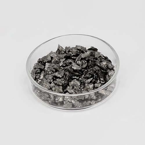
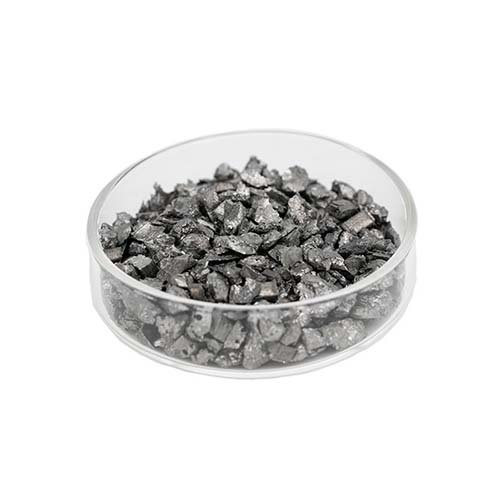
Erbium metal sputtering targets for thin film deposition are high-performance materials designed for advanced thin film deposition processes. The product has excellent density, which can ensure the uniformity and density of the deposited film, significantly improve the film quality and adhesion, and effectively reduce the impact of impurities on device performance. It is mainly used in semiconductors, displays, photovoltaics, and optical coatings.
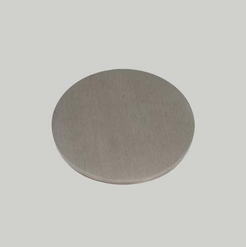
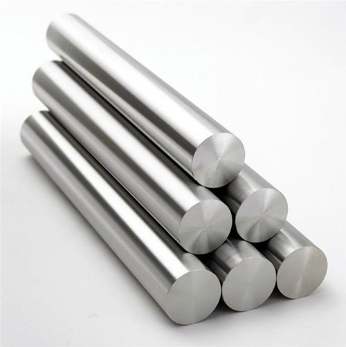
We provide high-quality Erbium metal sputtering targets for semiconductor applications in various specifications and shapes, including round, rectangular, and customized sizes to meet the diverse needs of customers in different processes and equipment. Whether it is used for scientific research and development or large-scale production, we can provide stable and high-quality product support with our Erbium metal sputtering targets for optical coating applications.
Product highlights of Erbium metal sputtering target
Excellent density, achieving uniform and dense film deposition
Various sizes and shapes, supporting personalized customization
Applicable to semiconductors, displays, photovoltaics and optical coatings
Support binding services
Applications of Erbium metal sputtering target
Semiconductor industry: Excellent conductivity and process compatibility make it an ideal material for interconnection and contact layers
Display manufacturing: Widely used in the reflective layer and electrode layer of LCD and OLED panels
Photovoltaic field: As the back electrode of thin-film solar cells, it improves cell efficiency and stability
Optical coating: Coating process for high reflectivity and functional optical components
Report
We provide detailed certificates of analysis (COA), material safety data sheets (MSDS) and related test reports for each batch of Erbium metal sputtering targets, support third-party authoritative testing, and ensure that product quality and performance reach world-class levels.
Molecular formula: Er
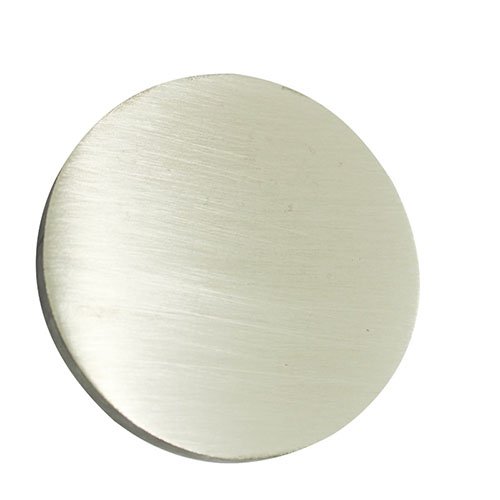
Appearance: Silvery white dense metal target with smooth and uniform surface
Density: about 9.07 g/cm³
Melting point: about 1,529 °C
Electrical conductivity: excellent metal conductivity
Crystal structure: hexagonal close-packed structure (HCP)
Chemical stability: stable in dry air and inert atmosphere, avoid high humidity environment
Corrosion resistance: good acid and alkali resistance, suitable for high temperature vacuum and extreme environment
Signal Word:
Danger Hazard Statements:
H228: Flammable solid
H260: In contact with water releases flammable gases which may ignite spontaneously
Inner packaging: Vacuum-sealed bag to protect against contamination and moisture.
Outer packaging: Carton or wooden box, depending on size and weight.
Fragile targets: Special protective packaging is used to ensure safe transport.


 Sputtering target- ULPMAT")