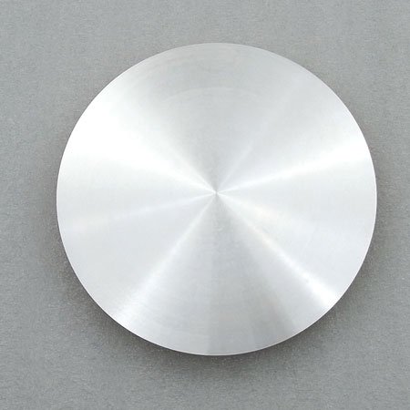
Copper Zinc Tin Selenide Sputtering Targets Overview
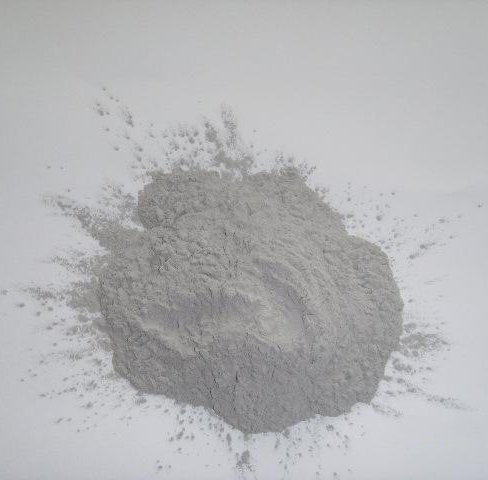
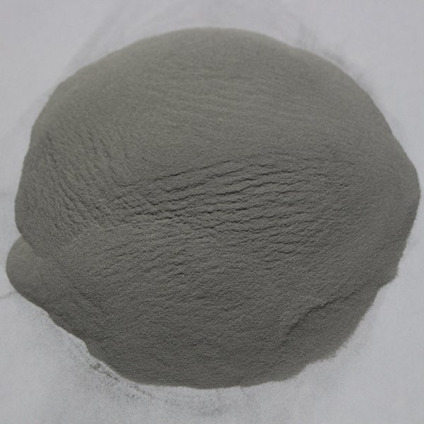
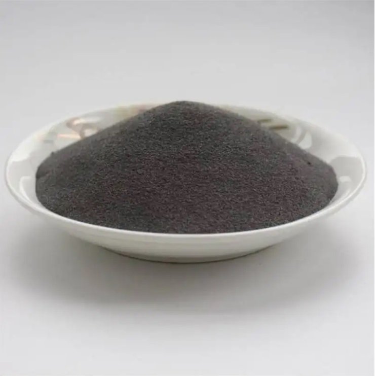
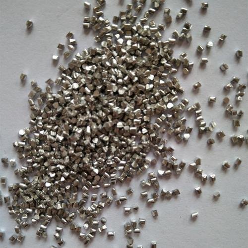
Copper Zinc Tin Selenide Sputtering Target is a key material used in physical vapor deposition (PVD) processes. It is precisely synthesized from high-purity copper, zinc, tin, and selenium elements in specific stoichiometric ratios, exhibiting excellent semiconductor properties and good light absorption characteristics. Cu2ZnSnSe4 targets are ideal for fabricating low-cost, high-efficiency, and environmentally friendly thin-film solar cell absorber layers, and are also suitable for other optoelectronic and semiconductor device applications.
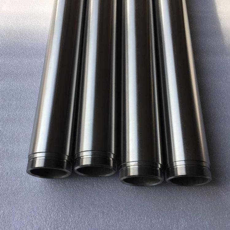
We offer a variety of high-purity, high-density Cu2ZnSnSe4 sputtering targets, supporting customized chemical compositions and sizes. Contact us.
Product Highlights
High Purity
Precise Stoichiometric Control
High Density, Low Porosity
Excellent Film Uniformity
Good Crystallization Performance
Environmentally Friendly Material
Supports Customized Production and Bonding
Applications of Cu2ZnSnSe4 Sputtering Targets
Thin-Film Solar Cells: Used as absorber layers to manufacture non-toxic, abundant next-generation thin-film photovoltaic devices.
Photodetectors: Used to manufacture photodetector elements sensitive to the visible to near-infrared region.
Semiconductor Devices: As a semiconductor active layer, it is used in display technology and logic circuits. Exploring potential materials for novel low-cost light-emitting devices.
Q1: What is the typical purity of Cu2ZnSnSe4 targets?
A1: The purity of our standard products is typically 99.99% (4N) or higher to ensure the stability and repeatability of thin film performance.
Q2: Can the size and composition of the targets be customized?
A2: Yes. We support customization of various diameters, thicknesses, and specific stoichiometry (such as copper-rich, zinc-rich, etc.) to meet your specific process requirements.
Q3: What is the conductivity type of Cu2ZnSnSe4 thin films?
A3: Cu2ZnSnSe4 typically exhibits p-type semiconductor behavior, but its conductivity type and carrier concentration can be optimized by adjusting the elemental stoichiometry and subsequent processes.
Q4: What are the advantages of Cu2ZnSnSe4 compared to other thin-film solar cell materials (such as CIGS)?
A4: Cu2ZnSnSe4 contains no rare (In) or toxic (Ga, Cd) elements. It boasts abundant raw material reserves, lower costs, and is more environmentally friendly, making it a more sustainable choice.
Report
Each batch is supplied with:
Certificate of Analysis (COA)
Technical Data Sheet (TDS)
Material Safety Data Sheet (MSDS)
Third-party testing reports available upon request
Why Choose Us?
We specialize in the production and supply of high-purity functional material sputtering targets, strictly controlling composition and batch stability. We provide reliable and traceable cuprous oxide sputtering targets for scientific research, industry, and electronic device thin film preparation, ensuring high-quality and long-term consistency of film deposition.


 Sputtering target- ULPMAT")