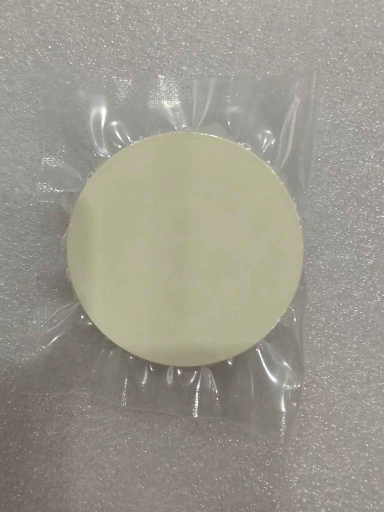
| Product ID | Formula | Purity | Dimension | Inquiry |
|---|---|---|---|---|
| 49083108300800ST001 | In2O3-Ga2O3-ZnO | 99.99% | Ø 50.8 mm x 3.175 mm | Inquire |
| 49083108300800ST002 | In2O3-Ga2O3-ZnO | 99.99% | Ø 50.8 mm x 6.35 mm | Inquire |
| 49083108300800ST003 | In2O3-Ga2O3-ZnO | 99.99% | Ø 76.2 mm x 3.175 mm | Inquire |
| 49083108300800ST004 | In2O3-Ga2O3-ZnO | 99.99% | Ø 101.6 mm x 4 mm | Inquire |
| 49083108300800ST005 | In2O3-Ga2O3-ZnO | 99.99% | Ø 101.6 mm x 6.35 mm | Inquire |
| 49083108300800ST006 | In2O3-Ga2O3-ZnO | 99.99% | Ø 152.4 mm x 3.175 mm | Inquire |
| 49083108300800ST007 | In2O3-Ga2O3-ZnO | 99.99% | Ø 152.4 mm x 6.35 mm | Inquire |
| 49083108300800ST008 | In2O3-Ga2O3-ZnO | 99.99% | Ø 203.2 mm x 3.175 mm | Inquire |
Indium-Gallium-Zinc Oxide (IGZO) is a ceramic oxide semiconductor composed of indium oxide (In₂O₃), gallium oxide (Ga₂O₃), and zinc oxide (ZnO). It is used to deposit thin films for thin-film transistors (TFTs), display backplanes, oxide semiconductor devices, and other electronic and optoelectronic applications. ULPMAT provides IGZO sputtering targets with an In₂O₃:Ga₂O₃:ZnO molar ratio of 1:1:1 and a purity of 99.99%.
Target quality should be evaluated beyond nominal purity. Composition, trace impurities, density, target dimensions, and batch consistency can affect sputtering behavior and deposited film performance. For a detailed discussion, see our article on IGZO sputtering target quality.
We supply high-quality oxide semiconductor targets for manufacturers and research institutions. Contact us for pricing and technical support.
| Parameter | Value |
| Product Name | IGZO Sputtering Target |
| Material | Indium Gallium Zinc Oxide |
| Composition | Customized |
| Purity | 99.99% |
| Representative Total Impurities | 37 ppm |
| Total Impurity Specification | ≤100 ppm |
| Representative Density | 6.42 g/cm³ |
| Target Type | Ceramic Sputtering Target |
The target has a specified purity of 99.99%. A representative finished-product inspection report recorded 99.99% measured purity and 37 ppm total tested impurities, compared with a specified limit of ≤100 ppm.
| Impurity | Specification | Measured Result |
| Co | ≤20 ppm | 12 ppm |
| Cu | ≤20 ppm | 8 ppm |
| Mn | ≤10 ppm | 6 ppm |
| Cr | ≤10 ppm | 3 ppm |
| Ni | ≤10 ppm | 5 ppm |
| Na | ≤10 ppm | 3 ppm |
| Total | ≤100 ppm | 37 ppm |
Analysis method: GDMS.
The reported values are based on the inspected batch. Actual results may vary by batch and should be confirmed against the applicable COA.
Thin-Film Transistors: Widely used as an oxide semiconductor material in TFT structures, it can be deposited by sputtering to form controlled thin films over large-area substrates.
Display Backplanes: The deposited films are used in oxide semiconductor backplane structures where switching characteristics and large-area film uniformity are important.
Oxide Semiconductor Devices: Suitable for research and development involving oxide semiconductor devices, thin-film transistors, and electronic materials.
Optoelectronic Applications: Its combination of optical transparency and semiconductor behavior makes it relevant to transparent and optoelectronic thin-film structures.
IGZO sputtering target is not defined by purity alone.A suitable target should provide controlled:
These factors should be evaluated together when selecting an IGZO sputtering target.For a more detailed explanation of how purity, composition, density, and microstructure affect target performance, see: IGZO Sputtering Target Quality: How Purity, Composition, and Density Affect Thin Film Performance.
How to Choose IGZO Sputtering Target: Key Specifications and Buying Guide
The target should first be selected according to the function of the deposited film and the configuration of the sputtering system.
Before purchasing, check:
If the intended application is still under evaluation, our comparison article IGZO vs ITO Sputtering Target explains when IGZO is more appropriate than ITO for different thin-film functions.
Technical documents can be provided according to the product and order requirements.
Download the TDS for detailed specifications.
Download the SDS for safety, handling, and storage information.
Custom specifications can be discussed according to equipment and deposition requirements, including:
For a custom target inquiry, provide the required composition, target dimensions, sputtering equipment information, and intended application.
Q1: What is an IGZO sputtering target?
A1: IGZO sputtering target is a ceramic oxide semiconductor target composed of indium oxide (In₂O₃), gallium oxide (Ga₂O₃), and zinc oxide (ZnO). It is used in sputter deposition to form thin films for thin-film transistors (TFTs), display backplanes, oxide semiconductor devices, and other electronic applications.
Q2: What is the composition of an IGZO sputtering target?
A2:The target described in the supplied finished-product inspection report has an indium oxide (In₂O₃), gallium oxide (Ga₂O₃), and zinc oxide (ZnO) molar ratio of 1:1:1. The exact composition should be confirmed against the product specification and inspection documentation for the specific target batch.
Q3: What is the purity of the IGZO sputtering target?
A3:The specified purity of this target is 99.99%, and the supplied finished-product inspection report records a measured purity of 99.99% for the inspected batch.
Q4: What are the impurity specifications for the IGZO target?
A4: The supplied inspection report specifies a total impurity limit of ≤100 ppm and records a measured total impurity level of 37 ppm for the inspected batch. Individual trace-element specifications should be confirmed using the corresponding inspection report or COA.
Q5:What is the density of the target?
A5:The supplied finished-product inspection report records a density of 6.42 g/cm³ for the inspected sample.
Q6: Can these sputtering targets be customized?
A6: Yes. These targets can be specified according to requirements such as composition ratio, purity, dimensions, thickness, geometry, and bonding configuration. The appropriate specification depends on the sputtering system and intended thin-film application.
Q7: What should I check before purchasing a target?
A7: Key parameters include In₂O₃:Ga₂O₃:ZnO composition, purity, trace impurities, total impurity level, density, dimensions, target geometry, bonding requirements, and quality documentation such as the TDS and COA. The target specifications should also match the requirements of the sputtering equipment.
Q8: Is IGZO the same as ITO?
A8: No. IGZO is an oxide semiconductor, while ITO is a transparent conductive oxide. IGZO is commonly used in TFT semiconductor layers, whereas ITO is widely used for transparent electrodes. For details, please read IGZO vs ITO Sputtering Target.
Chemical Formula: In₂O₃-Ga₂O₃-ZnO
Appearance: Off-white or silver-gray dense target
Crystal Structure: Amorphous/Microcrystalline
Binding Method: Customizable
Backing Plate Selection: Customizable
Sputtering Method: RF/DC Magnetron Sputtering
Inner Packaging: Vacuum-sealed bags and boxed to prevent contamination and moisture.
Outer Packaging: Cartons or wooden crates selected based on size and weight.
If you need any service, please contact us