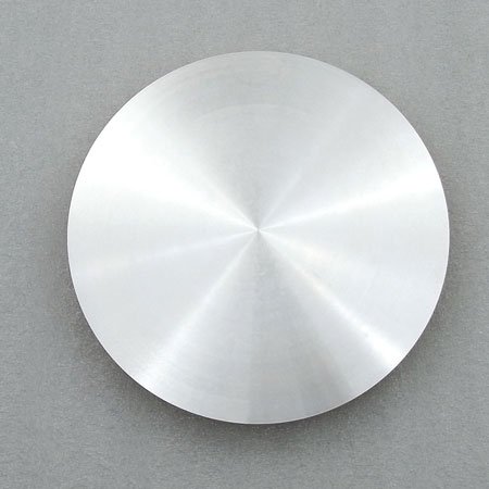
Tungsten Telluride sputtering targets are high-performance compound materials designed for advanced thin film deposition processes. They have excellent electrical and topological properties and are particularly suitable for the next generation of electronic devices and research fields. Their high purity and density ensure the formation of uniform and stable thin film structures, and exhibit excellent film quality and interlayer bonding.
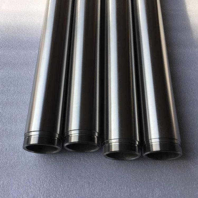
We can provide Tungsten Telluride targets in various shapes and sizes, including round, rectangular, etc., and can be customized according to your specific specifications. At the same time, we provide full technical support and after-sales service to assist customers in solving any problems encountered during use.
Purity: 99.95%
High density, uniform structure, and good thin film deposition effect
Standard sizes and customized services are available
Compatible with a variety of PVD processes (such as magnetron sputtering)
Applicable to topological insulator research, low-dimensional materials, two-dimensional devices and infrared detection
Topological electronic devices: WTe2 has topological fermion properties and is suitable for the development of new quantum materials and topological insulator devices.
Two-dimensional material research: Its layered structure is suitable for preparing thin layers or single layers of materials for low-dimensional electronics and optoelectronics.
Infrared detectors and sensors: WTe₂ thin films have good infrared response performance.
Spintronics: Used to study strong spin-orbit coupling effects and related quantum transport phenomena.
We provide complete quality inspection documents for each batch of products, including Certificate of Analysis (COA), Material Safety Data Sheet (MSDS) and necessary physical and chemical property reports. Support customers to entrust third-party testing to ensure objective and reliable data and stable and consistent products.
Molecular formula: WTe₂
Molecular weight: 447.3 g/mol
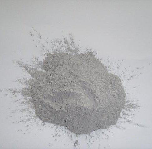
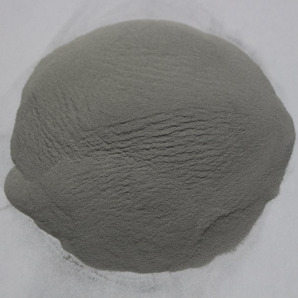
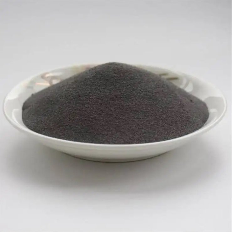
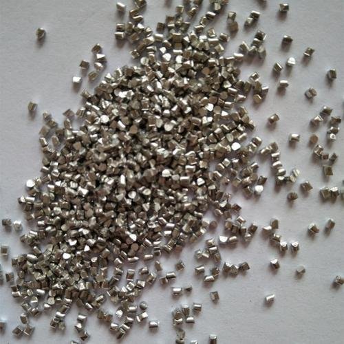
Appearance: Silver-grey metallic luster target, dense structure, smooth surface
Density: about 9.3 g/cm³ (close to theoretical density)
Melting point: about 1,200 °C (before decomposition)
Crystal structure: orthorhombic system (Td phase, with topological semi-metallic properties)
Inner Packaging: Vacuum-sealed bags and boxed to prevent contamination and moisture.
Outer Packaging: Cartons or wooden crates selected based on size and weight.
If you need any service, please contact us


 Sputtering target- ULPMAT")