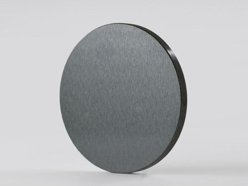
| Product ID | Formula | Purity | Dimension | Inquiry |
|---|---|---|---|---|
| 220500ST001 | TiB2 | 99.5% | Ø 50.8mm x 3.175mm | Inquire |
| 220500ST002 | TiB2 | 99.5% | Ø 50.8mm x 6.35mm | Inquire |
| 220500ST003 | TiB2 | 99.5% | Ø 101.6mm x 6.35mm | Inquire |
| 220500ST004 | TiB2 | 99.5% | Ø 202.3mm x 3.175mm | Inquire |
| 220500ST005 | TiB2 | 99.5% | Ø 202.3mm x 6.35mm | Inquire |
| 220500ST006 | TiB2 | 99.5% | 690*145*10mm | Inquire |
| 220500ST007 | TiB2 | 99.5% | 172.5*145*10mm | Inquire |
Titanium boride Sputtering Target is a high-hardness, high-melting-point ceramic sputtering target with excellent electrical conductivity and chemical stability. It is widely used in the development of high-hardness coatings, conductive ceramic films, functional thin films, and scientific thin film materials.
We offer TiB₂ sputtering targets with uniform composition and dense structure, suitable for DC or RF magnetron sputtering systems. Please contact us for detailed specifications and technical information.
High-hardness, high-melting-point ceramic target
Good electrical conductivity, stable thin film deposition
High temperature and corrosion resistance, strong thermal stability
Suitable for high-temperature, vacuum, and inert atmosphere deposition
High batch consistency
Customizable sizes and shapes
Suitable for scientific and industrial thin film preparation
High-hardness, wear-resistant coatings: Can be used to prepare wear-resistant, high-hardness coatings, widely used on the surfaces of cutting tools, molds, and industrial equipment.
Conductive Ceramic Films and Composite Films: Utilizing its conductivity and chemical stability, TiB2 can be used to prepare metal-ceramic composite films and conductive ceramic films for electronic devices and functional materials.
Research and Thin Film Development: Applicable to TiB2 functional thin film research, development of novel high-hardness coatings, and film performance testing.
High-Temperature Corrosion-Resistant Coatings: TiB2 films exhibit stability in high-temperature and corrosive environments, making them suitable for protective coatings and high-temperature electronic devices.
Q1: Which sputtering method is suitable for TiB2 targets?
A1: Suitable for DC magnetron sputtering and RF magnetron sputtering. It has good conductivity and is adaptable to various PVD processes.
Q2: Is the composition of TiB2 targets stable during sputtering?
A2: Under appropriate process conditions, the target maintains stable chemical composition, resulting in good film repeatability and consistency.
Q3: Are TiB2 targets suitable for high-temperature deposition?
A3: Yes, this target has excellent thermal stability and thermal shock resistance, making it suitable for high-temperature thin film deposition.
Q4: What are the main applications of TiB2 sputtering targets?
A4: Mainly used in the development of wear-resistant coatings, conductive ceramic films, functional films, and scientific research thin film materials.
For TiB₂ Sputtering Target, each batch is supplied with the following documentation:
Certificate of Analysis (COA) — Available upon request
Technical Data Sheet (TDS) — Download
Safety Data Sheet (SDS) — Download
Size Inspection Report (included with each shipment)
Third‑party testing reports available upon request
We focus on the research and supply of high-performance ceramic sputtering targets, ensuring that TiB2 sputtering targets meet scientific and industrial standards in terms of material structure, densification, and sputtering compatibility, providing reliable assurance for the preparation of functional thin films and high-hardness coatings.
Molecular Formula: TiB₂
Molecular Weight: 69.72 g/mol
Appearance: Black target material
Density: 4.5 g/cm³
Melting Point: Approx. 3225 °C
Crystal Structure: Hexagonal (P6₃/mmc)
Inner Packaging: Vacuum-sealed bags and boxed to prevent contamination and moisture.
Outer Packaging: Cartons or wooden crates selected based on size and weight.
If you need any service, please contact us