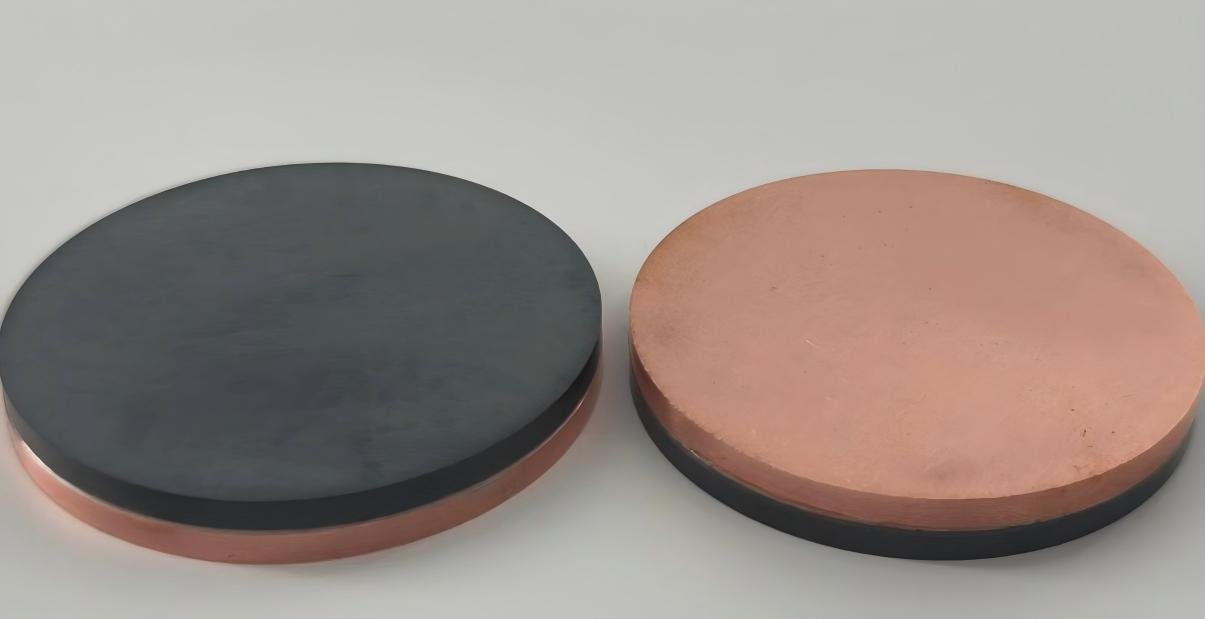
| Product ID | Formula | Purity | Dimension | Inquiry |
|---|---|---|---|---|
| 4908500800ST001 | In2O3-SnO2 (90/10 wt%) | 99.99% | Ø 50.8 mm x 3.175 mm | Inquire |
| 4908500800ST002 | In2O3-SnO2 (95/5 wt%) | 99.99% | Ø 50.8 mm x 6.35 mm | Inquire |
| 4908500800ST003 | In2O3-SnO2 (90/10 wt%) | 99.99% | Ø 76.2 mm x 6.35 mm | Inquire |
| 4908500800ST004 | In2O3-SnO2 (95/5 wt%) | 99.99% | Ø 101.6 mm x 4 mm | Inquire |
| 4908500800ST005 | In2O3-SnO2 (90/10 wt%) | 99.99% | Ø 101.6 mm x 6.35 mm | Inquire |
| 4908500800ST006 | In2O3-SnO2 (90/10 wt%) | 99.99% | Ø 152.4 mm x 3.175 mm | Inquire |
| 4908500800ST007 | In2O3-SnO2 (90/10 wt%) | 99.99% | Ø 152.4 mm x 6.35 mm | Inquire |
| 4908500800ST008 | In2O3-SnO2 (90/10 wt%) | 99.99% | Ø 203.2 mm x 3.175 mm | Inquire |
Indium Tin Oxide sputtering target (In2O3-SnO2) is a high-purity transparent conductive oxide (TCO) material widely used in thin film electronics, optoelectronic devices, and semiconductor applications. With excellent electrical conductivity, optical transparency, and uniform film formation, ITO sputtering targets are essential for manufacturing advanced displays, touch panels, solar cells, and other thin film devices. Our targets ensure 99.99% (4N) purity, dense structure, and stable performance for industrial and research applications.
We supply high-quality ITO sputtering targets for manufacturers and research institutions. Contact us for the best price and technical support.
Superior Purity: 99.99% (4N) purity meets stringent requirements for thin film and TCO applications.
High Performance: Excellent electrical conductivity and optical transparency for optoelectronic devices.
Stable Material: Dense structure, low impurity content, and uniform composition ensure reproducible thin film results.
Flexible Sizes: Available in various dimensions to suit different deposition systems.
Thin Film Electronics: Applied in transparent electrodes, thin film transistors (TFTs), and OLED displays.
Optoelectronic Devices: Used in touch panels, photodetectors, infrared sensors, and flexible electronics.
Solar Cells: Suitable for transparent electrode layers in advanced CIGS and perovskite solar cells.
Research and Development: Widely used in laboratories for material science and device research.
Energy Devices: Applied in transparent conductive films for energy conversion and storage applications.
Industry Expertise: Specialized in high-purity sputtering targets for TCO and thin film technologies.
Customized Solutions: Flexible in target composition, dimensions, and backing plate selection.
Reliable Quality: Strict impurity control, dense structure, and uniform composition ensure stable performance.
Global Delivery: Fast, secure shipping worldwide with protective packaging.
Technical Support: Professional team provides full technical documentation and consultation.
1. What is an Indium Tin Oxide (ITO) Sputtering Target?
An Indium Tin Oxide (ITO) Sputtering Target is a ceramic target material made from indium oxide (In₂O₃) and tin oxide (SnO₂) used for physical vapor deposition (PVD) processes. During sputtering, ITO targets are used to deposit transparent conductive oxide (TCO) thin films with high electrical conductivity and optical transparency for advanced electronic and optoelectronic applications.
2. What is the composition of an ITO Sputtering Target?
ITO Sputtering Targets are typically composed of indium oxide (In₂O₃) and tin oxide (SnO₂). The most commonly used composition is approximately 90 wt% In₂O₃ and 10 wt% SnO₂, although different compositions may be selected depending on the required electrical, optical, and deposition properties of the final thin film.
3. What are ITO Sputtering Targets used for?
ITO Sputtering Targets are widely used to produce transparent conductive films for flat panel displays, touch panels, photovoltaic devices, OLED-related technologies, sensors, and other optoelectronic applications. ITO films are valued because they combine high visible light transparency with good electrical conductivity.
4. Why is ITO used as a transparent conductive material?
ITO is widely used as a transparent conductive material because it provides a combination of high optical transparency and electrical conductivity. The tin doping in In₂O₃ improves electrical carrier concentration while maintaining the optical properties required for transparent electrodes in electronic devices.
5. What purity is available for ITO Sputtering Targets?
ITO Sputtering Targets are available in high-purity grades, commonly including 99.99% purity, depending on application requirements. High purity helps minimize impurity-related defects during thin-film deposition and supports stable sputtering performance for demanding optoelectronic applications.
6. How do I choose an ITO Sputtering Target?
When choosing an ITO Sputtering Target, consider the In₂O₃/SnO₂ composition ratio, purity, target density, dimensions, thickness, target shape, bonding configuration, sputtering equipment, and required film properties. Target density, microstructure uniformity, and composition consistency can influence sputtering stability and deposited film performance.
7. What shapes and sizes are available for ITO Sputtering Targets?
ITO Sputtering Targets are available in different configurations, including planar and rotary targets, depending on sputtering equipment requirements. Custom dimensions, thicknesses, bonding options, and backing plate configurations can be provided for laboratory, research, and industrial thin-film deposition systems.
8. Can ITO Sputtering Targets be customized?
Yes. ITO Sputtering Targets can be customized according to composition ratio, purity, dimensions, density requirements, target geometry, bonding method, and sputtering system specifications. Customized solutions are available for display, photovoltaic, semiconductor, optical coating, and research applications.
Each batch of products is supplied with:
Certificate of Analysis (COA)
Technical Data Sheet (TDS)
Material Safety Data Sheet (MSDS)
Third-party testing reports are available upon request to meet industrial and research standards.
Molecular Formula: In₂O₃-SnO₂
Appearance: Off-white or silver-gray dense target
Melting Point: ~1900°C
Boiling Point: ~2000°C
Crystal Structure: Cubic (In₂O₃ as the primary phase)
Inner Packaging: Vacuum-sealed bags and boxed to prevent contamination and moisture.
Outer Packaging: Cartons or wooden crates selected based on size and weight.
If you need any service, please contact us