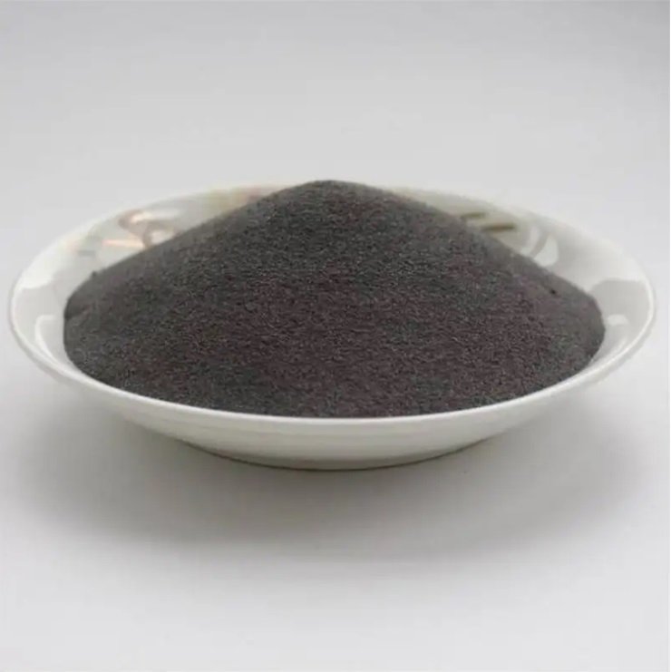
Indium Metal Sputtering Target Overview
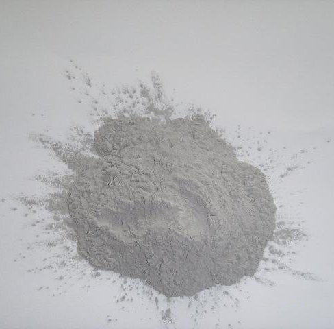
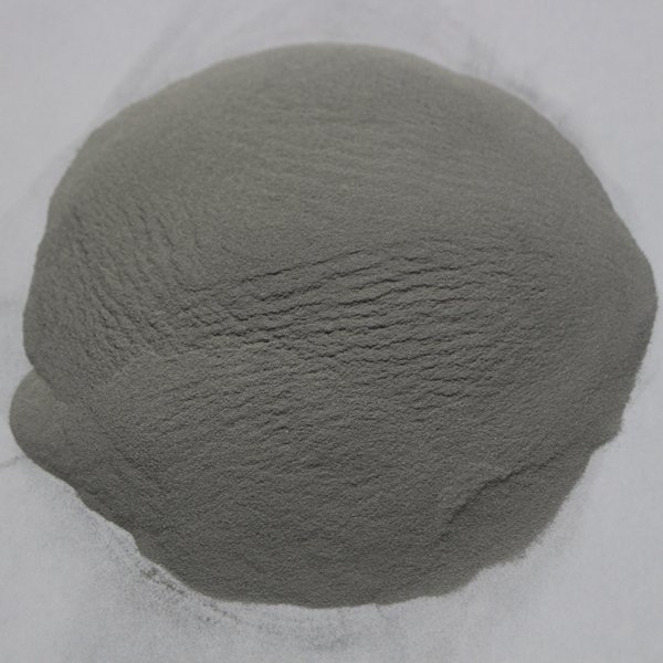
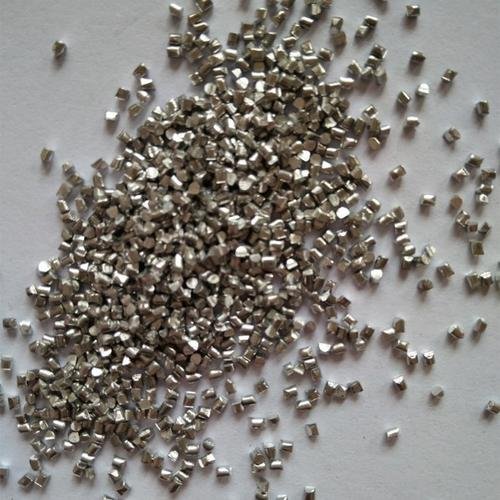
Indium (In) metal sputtering targets are high-purity metallic materials widely used in thin film deposition, optoelectronics, and advanced semiconductor applications. With excellent ductility, low melting point, and outstanding conductivity, indium targets are the preferred choice for PVD processes, especially in transparent conductive coatings, low-temperature soldering films, and microelectronic device fabrication.
Our indium metal sputtering targets feature 99.99% (4N) to 99.999% (5N) purity, high density, and uniform microstructure, ensuring consistent performance in both industrial production and scientific research.
Product Highlights of Indium Sputtering Target
High Purity: 99.99% (4N)–99.999% (5N) for stable thin film quality and minimal impurities.
Excellent Workability: Soft, ductile metal with reliable film-forming properties.
Uniform Density: Optimized for consistent sputtering rates and uniform coating thickness.
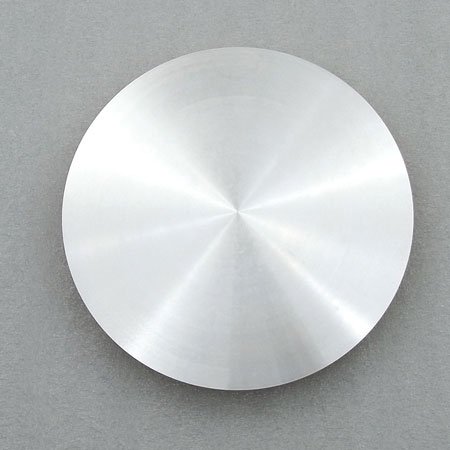
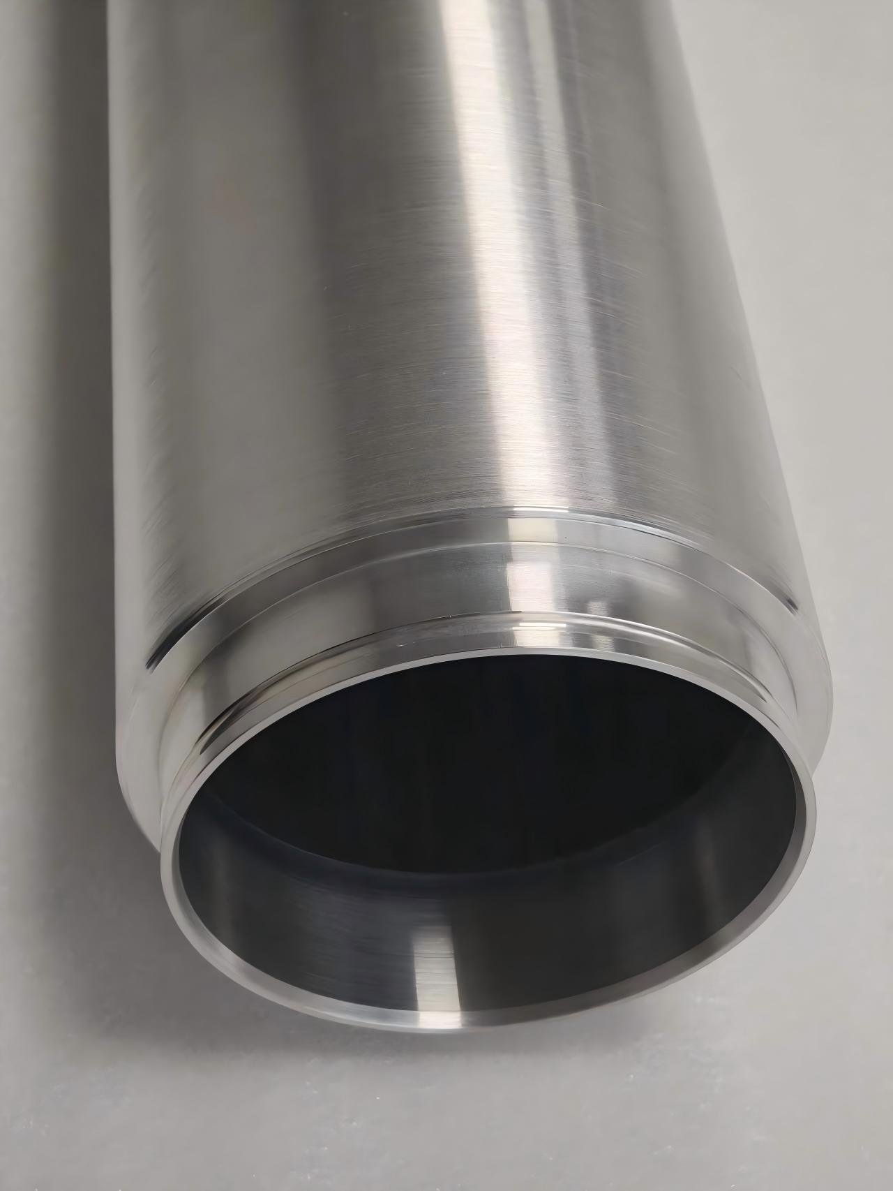
Wide Size Options: Available in planar, rotary, and custom shapes.
Stable Supply: Suitable for high-volume production and laboratory research.
Applications of In Sputtering Target
Transparent Conductive Coatings: Essential for display panels, OLED, LCD, and solar cells.
Semiconductor Fabrication: Used in low-temperature soldering and interconnect materials.
Optoelectronics: Applied in thin film transistors, photodetectors, and infrared devices.
Energy Materials: Suitable for electrode and thin film battery R&D.
Scientific Research: Extensively used in universities and laboratories for materials science.
Why Partner with Us?
Material Expertise: Years of experience in metallic sputtering targets.
Custom Solutions: Flexible sizes, shapes, and purities to meet project requirements.
Quality Control: ICP-MS impurity analysis for every production batch.
Reliable Logistics: Secure packaging and on-time delivery worldwide.
Technical Support: Professional team to assist in your thin film development.
F1. What are the advantages of indium sputtering targets compared to indium pellets or wire?
A1. Targets ensure higher density, uniform sputtering rates, and improved thin film quality.
F2. What purity grades are available?
A2. We provide 4N (99.99%) and 5N (99.999%) purities, with custom grades available on request.
F3. Can indium targets be bonded?
A3. Yes, indium targets can be bonded to backing plates (copper, molybdenum, titanium) for enhanced stability.
F4. How are indium metal sputtering targets packaged?
A4. Targets are vacuum-sealed with protective cushioning, shipped in rigid export-safe cartons.
F5. Which industries mainly use indium metal sputtering targets?
A5. They are widely applied in display technology, optoelectronics, semiconductors, and renewable energy sectors.
Reports
Each batch is supplied with:
Certificate of Analysis (COA)
Technical Data Sheet (TDS)
Material Safety Data Sheet (MSDS)
Third-party testing reports available upon request


 Sputtering target- ULPMAT")