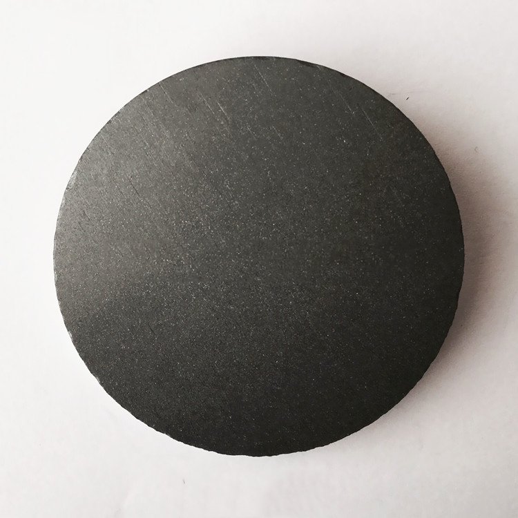
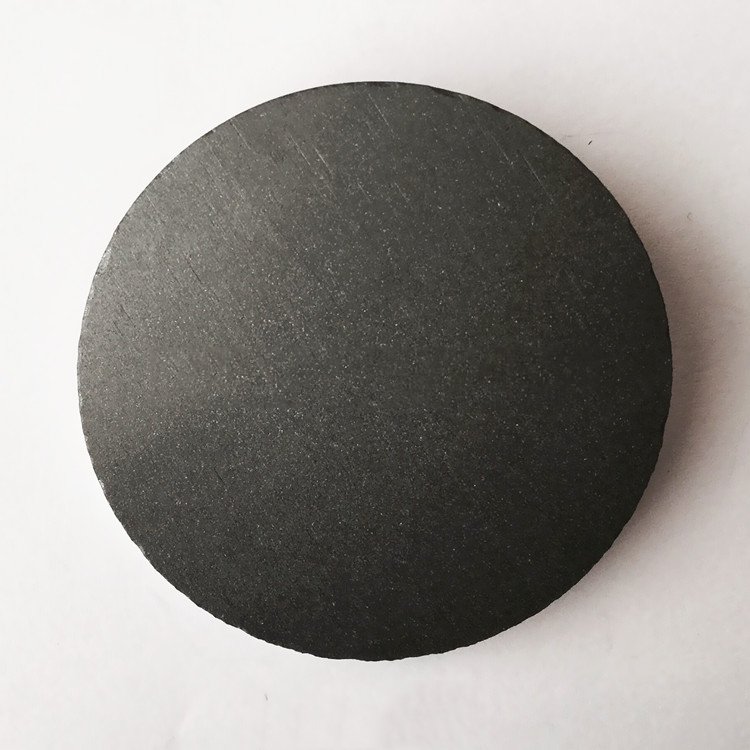
Cadmium Telluride Sputtering Targets Overview
Cadmium Telluride sputtering targets are high-performance materials used in optoelectronic thin film deposition, possessing excellent light absorption and stable semiconductor properties. They are commonly used to prepare functional thin films such as thin-film solar cells, optical components, infrared detectors, and transparent electrode layers, making them an indispensable core material in the optoelectronic industry and research fields.
We offer CdTe sputtering targets ranging from high purity and custom sizes to single-crystal/polycrystalline structures, supporting full customization in diameter, thickness, purity, and backplane type. Please contact us for quotations, technical parameters, or samples.
Product Highlights
High-purity material with extremely low impurity content
High density and excellent sputtering stability
Excellent uniformity and high-quality films
Multiple sizes and backplane options available
Target bonding services available
Compatible with mainstream vacuum deposition equipment
Mass production customization available
Stable optical and electrical properties of the thin films
Applications of Cadmium Telluride Sputtering Targets
Used for preparing absorption layers in high-efficiency thin-film solar cells.
Used in functional thin films for infrared photodetectors and optoelectronic sensors.
Used for depositing uniform CdTe semiconductor thin films in optical coating and materials research.
1. What is Cadmium Telluride Sputtering Target?
Cadmium Telluride Sputtering Target is a CdTe-based deposition material used to produce thin films through sputtering processes. It is commonly evaluated for semiconductor research, photovoltaic devices, and optical applications.
2. What are CdTe sputtering targets used for?
CdTe sputtering targets are mainly used for thin film deposition, including semiconductor devices, photovoltaic materials, optical coatings, and advanced material research.
3. What is the chemical formula of Cadmium Telluride?
The chemical formula of Cadmium Telluride is CdTe, consisting of cadmium and tellurium in a 1:1 atomic ratio. The molecular weight is approximately 240.01 g/mol.
4. What purity options are available for CdTe targets?
ULPMAT supplies CdTe targets with different purity levels according to application requirements. Purity, dimensions, and target configurations can be customized based on customer specifications.
5.Which sputtering process is suitable for CdTe target materials?
CdTe target materials are commonly used in physical vapor deposition (PVD) processes, including RF sputtering systems. The suitable process depends on equipment configuration and film requirements.
6. Can ULPMAT provide customized CdTe sputtering targets?
Yes. ULPMAT provides customized solutions including target size, shape, thickness, and bonding options according to customer equipment and deposition requirements.
7. How should Cadmium Telluride targets be stored and handled?
Cadmium Telluride targets should be stored in a dry and clean environment with suitable protection against mechanical damage. Proper handling procedures and personal protective equipment should be followed according to the SDS.
8. What documents are available for CdTe target evaluation?
ULPMAT can provide technical documents including SDS, TDS, and quality-related documents to support material evaluation and research applications.
Reports
Each batch is supplied with:
Certificate of Analysis (COA)
Technical Data Sheet (TDS)
Material Safety Data Sheet (MSDS)
Third-party testing reports available upon request
Why Choose Us?
We possess mature target sintering processes, a precise quality control system, and a stable supply chain, enabling us to provide high-density, high-purity CdTe targets with excellent sputtering stability. Our engineering team can provide process optimization suggestions, customized manufacturing, and rapid global delivery, offering reliable and highly consistent thin film material solutions for research institutions and optoelectronic manufacturing companies. We are a trusted supplier in the optoelectronic thin film industry.