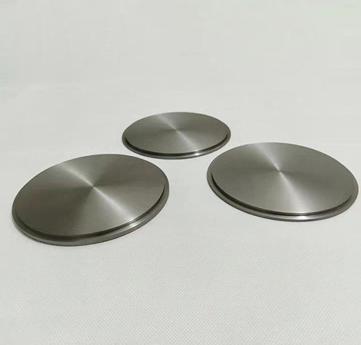
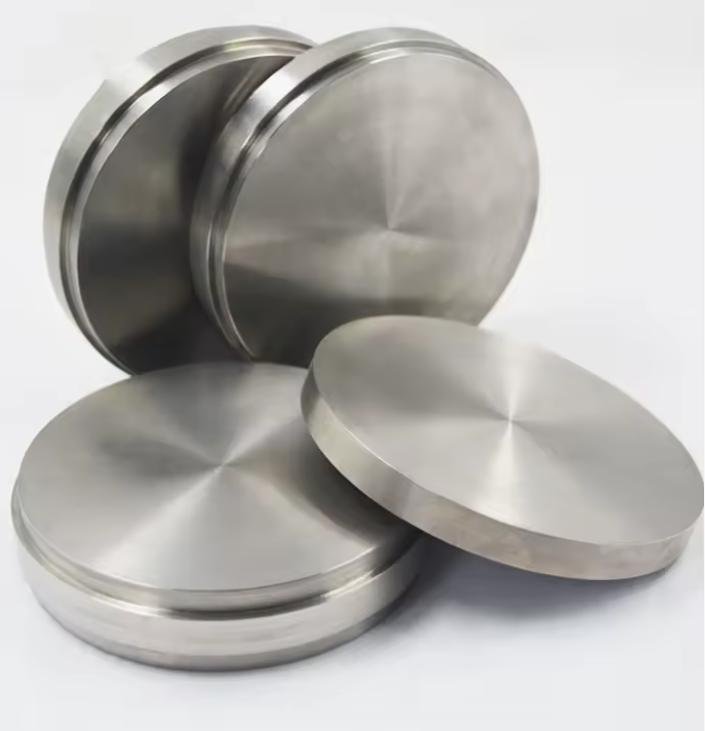
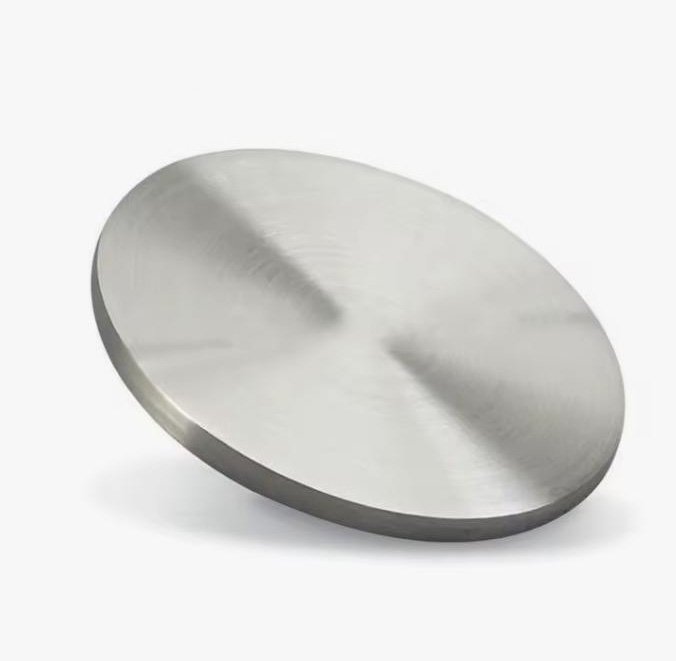
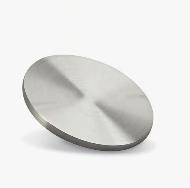
Sputtering Targets Overview
Sputtering targets are core components in the sputtering process, bombarded by high-speed ion beams to provide source atoms for thin film deposition. In Physical Vapor Deposition (PVD) used in electronic manufacturing, high-purity sputtering targets are vital. They enable production of electronic thin films on wafers, displays, solar cells, and other advanced equipment.
Simply put, sputtering targets are the “raw materials” in a microscopic metal transfer process. High-energy particles strike the target, ejecting (“sputtering”) atoms that deposit on substrates to form thin films.
Classification of Sputtering Targets
By material type:
- Metal Targets: Pure metals like silicon, aluminum, titanium, tungsten, etc.
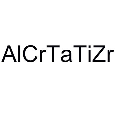
- Alloy Targets: Metal combinations, e.g., tungsten-molybdenum, titanium-aluminum alloys.
- Ceramic Targets: Non-metallic compounds like aluminum oxide (Al₂O₃), zinc oxide (ZnO), indium tin oxide (ITO).
- Composite Targets: Multi-element materials including nitrides, carbides, sulfides, silicides.
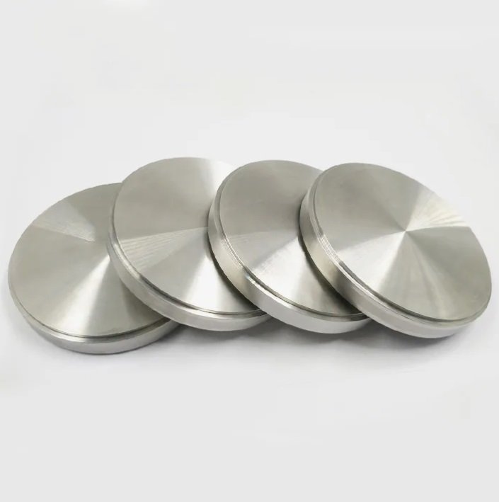
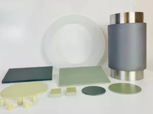
By shape and structure:
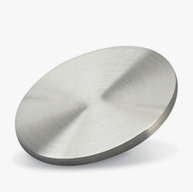
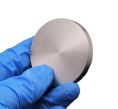
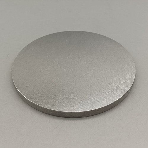
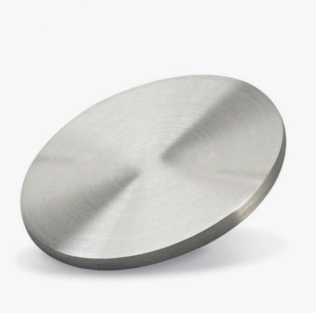
- Planar Targets: Circular, rectangular, triangular, ring-shaped, and custom shapes; commonly used in magnetron sputtering.
- Rotary Targets: Cylindrical targets that rotate during sputtering to improve utilization and film uniformity.
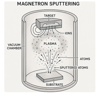
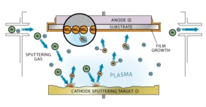
How Sputtering Targets Work
Gas Ionization: Argon gas in vacuum is ionized by high voltage to produce ions.
Ion Bombardment: Ions accelerate and strike the target surface, ejecting atoms from its lattice.
Thin Film Deposition: Ejected atoms travel and deposit onto substrate, forming a thin film.
Performance Requirements for Sputtering Targets
- Purity: ≥99.9% to ensure deposited film quality and performance.
- Density: High density reduces contamination, improves film uniformity.
- Chemical Composition Uniformity: Ensures stable deposited film properties.
- Crystal Structure: Proper structure enhances sputtering efficiency and film quality.
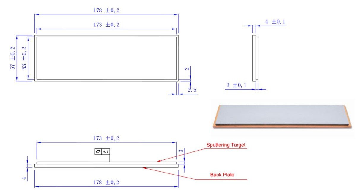
- Size and Shape Accuracy: Must meet equipment requirements for good installation and effect.
- Thermal Stability: Target endures high temperature and energetic particles.
- Corrosion Resistance: Extends service life of the target material.
Sputtering Target Fabrication Processes
- Melting and Casting
Materials: Metals and some alloys.
Process: High-purity metals melted under vacuum or inert atmosphere and cast.
Pros: Low cost, mass production, uniform composition, large targets.
Cons: Not for high melting or oxidation-sensitive metals (e.g. Ti, W, Mo), lower density.
Applications: Aluminum, copper, chromium targets.

- Powder Metallurgy (PM)
Materials: Metals, alloys, ceramics, composites.
Process: Powders mixed, compacted (e.g. CIP), sintered at high temperature.
Pros: Ideal for high melting or complex materials, high purity and density, flexible composition.
Cons: Strict atmosphere and temperature control needed.
Applications: Ceramic (Al₂O₃, ZnO, TiO₂), alloy (Ti-Al, Cr-Ni) targets.
- Hot Isostatic Pressing (HIP)
Materials: Metals, alloys, ceramics.
Process: Powders densified under high temperature and pressure.
Pros: Very dense targets with excellent properties.
Cons: Expensive; not ideal for oxidation-sensitive materials.
Applications: Nitride, oxide, boride ceramics, high-performance composites.
- Spark Plasma Sintering (SPS)
Materials: High-entropy alloys, ceramics, metal compounds.
Process: Fast sintering using pulsed electric current and pressure.
Pros: Short time, minimal grain growth, good composition retention.
Cons: High equipment cost, suited for lab or small batches.
Applications: High-performance or research-grade ceramic and alloy targets.
- Cold Pressing + Hot Sintering
Materials: Metals, ceramics, composites.
Process: Powders cold-pressed, then sintered in vacuum or inert gas.
Pros: Simple, lower cost than SPS, easy size/shape control.
Cons: Density lower than HIP, better for small/medium targets.
Applications: Standard metal, alloy, ceramic targets.
Properties of Sputtering Targets
- Purity: Minimizes impurities that affect thin film properties.
- Density: Enhances sputtering efficiency and reduces porosity.
- Electrical & Thermal Conductivity: Ensures process stability.
- Corrosion Resistance & Thermal Stability: Reliable performance under extreme conditions.
Applications of Sputtering Targets
Semiconductors: Metal and dielectric films to enhance IC performance.
Displays: LCD, PDP, OLED manufacturing for transparent conductive and emissive layers.
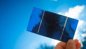
Solar Cells: Forming silicon and CIGS thin films to improve efficiency.
Optics: Anti-reflective, reflective, and filter coatings for lenses and instruments.
Aerospace: Protective and wear-resistant coatings for durability in harsh environments.
Contact us today to discuss your sputtering target needs — let us help you achieve exceptional thin film results.