
Semiconductor Materials
Enabling Next-Gen Devices with High Purity and Reliability
Semiconductor Materials
Semiconductor materials, refers to room temperature conductivity between the conductor and insulator between the material, it has specific electrical and physical properties, these properties make the semiconductor device circuit has a unique performance, one of the characteristics of its doping process can be used to add a specific element to change and control their Electrical properties, can be used as a component material for information processing.
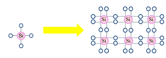
Intrinsic semiconductor refers to those very pure single-crystal semiconductors, the manufacture of semiconductor materials required for the very high purity, usually up to 99.9999999%(9N). These materials appear as single crystals in their physical structure, and single-crystal silicon (Si) and single-crystal germanium (Ge) are commonly used semiconductor materials.
By doping intrinsic semiconductors with trace amounts of impurities (a process known as doping), we can significantly change the conductivity of a semiconductor. The intrinsic semiconductor that has been doped is called an impurity semiconductor. Depending on the type of impurity doped (mainly trivalent or pentavalent elements), semiconductors are classified into two broad categories: p-type and n-type.
N-Type Semiconductors
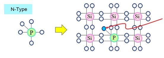
N-type semiconductors are made by doping intrinsic semiconductors, such as silicon, with pentavalent elements such as phosphorus P, arsenic As, and antimony Sb. These elements have one more valence electron than silicon and will provide additional free electrons.
Key features:
Doped elements: phosphorus (P), arsenic (As), antimony (Sb), etc.
Excess free electrons (negative carriers)
Increase in the number of free electrons, increase in conductivity
Direction of current is mainly determined by the movement of electrons
P-type semiconductor
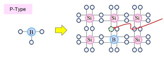
P-type semiconductors are made by doping intrinsic semiconductors with trivalent elements such as boron B, aluminium Al, and gallium Ga. These elements have one less valence electron than silicon and leave holes in the lattice.
Key features:
Dopant elements: boron (B), aluminium (Al), gallium (Ga), etc.
Holes (positive carriers)
Hole as carriers involved in the conductive
The direction of current is mainly determined by the movement of holes
Classification of semiconductors:
Elemental semiconductors
Silicon (Si): the most widely used, accounting for more than 90% of the semiconductor industry, used in integrated circuits, solar cells, etc..
Germanium (Ge): the main material of the early semiconductor devices, now used in high-frequency circuits and infrared optical devices.
Compound semiconductors
III-V compounds: such as gallium arsenide (GaAs), indium phosphide (InP), with high electron mobility, suitable for high-frequency communications, optoelectronic devices (lasers, LEDs).
Wide-band semiconductors:
Silicon Carbide (SiC): high temperature and high voltage resistant, used in electric vehicles, power electronics.
Gallium Nitride (GaN): excellent high-frequency performance, used in 5G base stations, fast charging devices.
II-VI compounds: such as cadmium telluride (CdTe), zinc sulfide (ZnS), mainly used in infrared detectors and photovoltaic field.
Material Characteristics and Applications
Generational Classification of Semiconductor Materials
| Generation | Representative Materials | Characteristics | Typical Applications |
|---|---|---|---|
| 1st Gen | Silicon (Si), Germanium (Ge) | Mature and well-established Low cost Easy to process Moderate thermal conductivity | Integrated circuits (ICs) Transistors Diodes General electronics |
| 2nd Gen | Gallium Arsenide (GaAs), Indium Phosphide (InP) | High electron mobility High-frequency performance Good for optoelectronics Higher production cost | RF communication Microwave devices Photodetectors GPS Navigation |
| 3rd Gen | Gallium Nitride (GaN), Silicon Carbide (SiC), Zinc Oxide (ZnO), Zinc Selenide (ZnSe) | Wide bandgap High breakdown voltage High thermal conductivity High-frequency, high-efficiency High-temperature tolerance | 5G base stations Electric vehicles Lasers Power electronics (IGBT/MOSFET) |
| 4th Gen | Gallium Oxide (Ga2O3), Diamond (C), Aluminum Nitride (AlN), Boron Nitride (BN) | Ultra-wide bandgap High carrier mobility High breakdown field strength Emerging and under development | Next-gen high-voltage power devices Aerospace Electronics for extreme environments (radiation/high temperature) |
ULPMAT has many years of experience in the field of semiconductor materials, with state-of-the-art production facilities and proven expertise. We are committed to providing high-performance, cutting-edge materials to meet your specific needs.
Contact us
More Information
- PHONE:+86-29-88993870
- WHATSAPP:+8618291498609
- E-MAIL:sales@ulpmat.com
- ADDRESS:A11, 5th Floor, Building 5, Digital China Xi’an Science Park, No. 20 Zhangba 4th Road, High-tech Zone, Xi’an, Shaanxi, China.
