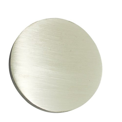
Ytterbium fluoride sputtering targetis a high-performance rare earth fluoride material specially designed for thin film deposition processes. With a purity of up to 99.99%, uniform and dense density, it ensures uniform film formation, strong adhesion, and extremely low impurity content, providing a solid guarantee for the preparation of high-end optoelectronics and functional materials.
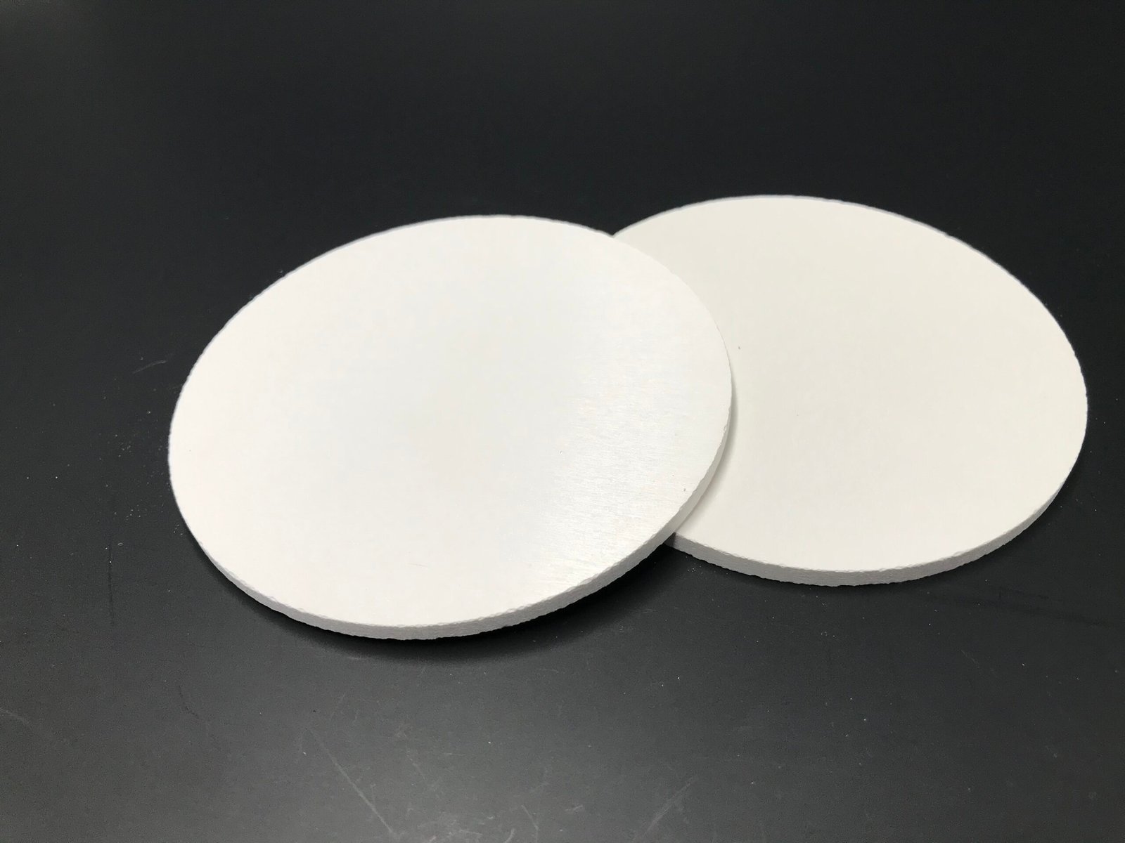
We provide Ytterbium fluoride sputtering target of various specifications and sizes, supporting circular and rectangular customization to meet your different process requirements. Our high-purity Ytterbium fluoride sputtering target is ideal for advanced thin film deposition and optoelectronic applications. The professional after-sales service team is always available to answer your technical questions and ensure that you can use it without worries.
Product Highlights of Ytterbium Fluoride sputtering target
The purity is as high as 99.99%, meeting the needs of scientific research and industrial-grade thin films
Dense and high-density structure ensures uniform deposition and excellent adhesion of thin films
Supports customization of multiple sizes and shapes, suitable for different sputtering equipment
Excellent thermal stability and chemical stability, suitable for a variety of vacuum sputtering processes
Applications of Ytterbium Fluoride sputtering target
Semiconductor:Ytterbium Fluoride sputtering targetused for the preparation of functional thin films for high-performance electronic devices to improve device stability and performance.
Optical coating: used to manufacture high-refractive index, low-absorption anti-reflection films and infrared window coatings.
Laser materials: Thin film sources of laser doping materials for near-infrared lasers and optical communication devices.
Optoelectronic devices: Preparation of thin film layers with special optical and electrical properties for new display and sensor fields.
Reports
We provide Certificate of Analysis (COA), Material Safety Data Sheet (MSDS) and other relevant reports for each batch of goods. In addition, we also support third-party testing for enhanced quality assurance.
Molecular Formula: YbF₃
Molecular Weight: 123 g/mol
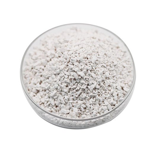
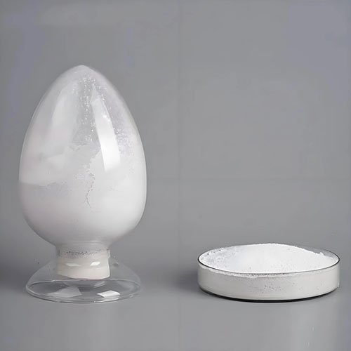
Appearance: White, dense ceramic target with a smooth surface
Density: Approximately 7.1 g/cm³ (close to theoretical density)
Melting Point: Approximately 1,230°C
Conductivity: Electrical insulator (high resistance)
Crystal Structure: Orthorhombic
Chemical Stability: Stable in dry air and inert atmospheres, low hygroscopicity
Signal Word:
Danger Hazard Statements:
H302+H312: Harmful if swallowed or in contact with skin
H331: Toxic if inhaled
H335: May cause respiratory irritation
H315: Causes skin irritation
H319: Causes serious eye irritation
Inner packaging: Vacuum-sealed bag to protect against contamination and moisture.
Outer packaging: Carton or wooden box, depending on size and weight.
Fragile targets: Special protective packaging is used to ensure safe transport.


 Sputtering target- ULPMAT")