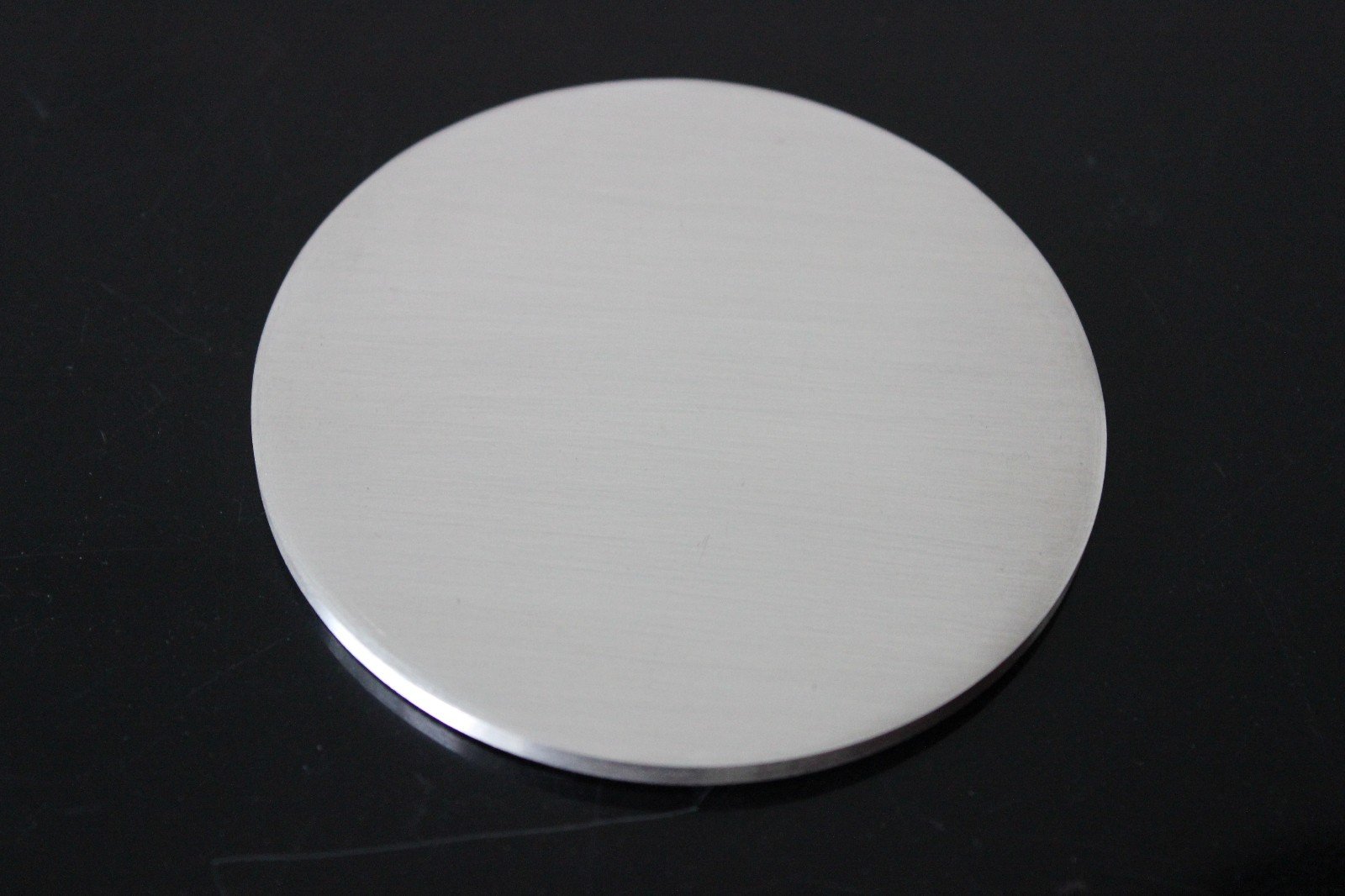
| Product ID | Formula | Purity | Dimension | Inquiry |
|---|---|---|---|---|
| 4900ST001 | In | 99.99% | Ø 25.4 mm x 6.35 mm | Inquire |
| 4900ST002 | In | 99.999% | Ø 25.4 mm x 6.35 mm | Inquire |
| 4900ST003 | In | 99.99% | Ø 50.8 mm x 6.35 mm | Inquire |
| 4900ST004 | In | 99.999% | Ø 50.8 mm x 6.35 mm | Inquire |
| 4900ST005 | In | 99.99% | Ø 76.2 mm x 6.35 mm | Inquire |
| 4900ST006 | In | 99.999% | Ø 76.2 mm x 6.35 mm | Inquire |
Indium (In) metal sputtering targets are high-purity metallic materials widely used in thin film deposition, optoelectronics, and advanced semiconductor applications. With excellent ductility, low melting point, and outstanding conductivity, indium targets are the preferred choice for PVD processes, especially in transparent conductive coatings, low-temperature soldering films, and microelectronic device fabrication.
Our indium metal sputtering targets feature 99.99% (4N) to 99.999% (5N) purity, high density, and uniform microstructure, ensuring consistent performance in both industrial production and scientific research.
High Purity: 99.99% (4N)–99.999% (5N) for stable thin film quality and minimal impurities.
Excellent Workability: Soft, ductile metal with reliable film-forming properties.
Uniform Density: Optimized for consistent sputtering rates and uniform coating thickness.
Wide Size Options: Available in planar, rotary, and custom shapes.
Stable Supply: Suitable for high-volume production and laboratory research.
Transparent Conductive Coatings: Essential for display panels, OLED, LCD, and solar cells.
Semiconductor Fabrication: Used in low-temperature soldering and interconnect materials.
Optoelectronics: Applied in thin film transistors, photodetectors, and infrared devices.
Energy Materials: Suitable for electrode and thin film battery R&D.
Scientific Research: Extensively used in universities and laboratories for materials science.
Material Expertise: Years of experience in metallic sputtering targets.
Custom Solutions: Flexible sizes, shapes, and purities to meet project requirements.
Quality Control: ICP-MS impurity analysis for every production batch.
Reliable Logistics: Secure packaging and on-time delivery worldwide.
Technical Support: Professional team to assist in your thin film development.
1. What is an Indium Sputtering Target?
An Indium Sputtering Target is a high-purity metallic indium material used as a source material for thin-film deposition by sputtering. It is used in PVD processes to deposit indium-containing films for semiconductor, optoelectronic, display, photovoltaic, and other functional thin-film applications.
2. What purity is available for Indium Sputtering Targets?
Indium Sputtering Targets are available in different purity grades, including 99.99%, and 99.999% grades, depending on the application and impurity-control requirements. Higher-purity indium can help reduce contamination during thin-film deposition and is generally preferred for applications with strict material purity requirements.
3. What are Indium Sputtering Targets used for?
Indium Sputtering Targets are used for thin-film deposition in semiconductor, optoelectronic, display, LED, photovoltaic, optical, and functional coating applications. They can also be used to deposit indium-containing films for research and development. The final film properties depend on the target purity, substrate, sputtering system, and deposition conditions.
4. How do I choose an Indium Sputtering Target?
When choosing an Indium Sputtering Target, consider the required purity, target shape and dimensions, sputtering equipment, bonding configuration, and intended thin-film application. The target should be compatible with the cathode and substrate system while providing the required impurity control and deposition performance. For custom targets, the equipment specifications and required target dimensions should be confirmed before production.
5. Can Indium Sputtering Targets be customized?
Yes. Indium Sputtering Targets can be customized according to the required purity, dimensions, thickness, shape, and sputtering equipment. Depending on the application, options can include planar or other target configurations, custom dimensions, and bonding or backing-plate requirements. Custom specifications should be confirmed based on the customer’s deposition system and application requirements.
6. What shapes and sizes are available for Indium Sputtering Targets?
Indium Sputtering Targets are available in various shapes and dimensions, including circular and rectangular configurations. Standard sizes may include different diameters and thicknesses, while custom sizes can be produced according to the sputtering equipment requirements. Target dimensions, thickness, mounting configuration, and other specifications should be confirmed before ordering.
Each batch is supplied with:
Certificate of Analysis (COA)
Technical Data Sheet (TDS)
Material Safety Data Sheet (MSDS)
Third-party testing reports available upon request
Chemical formula: In
Atomic weight: 114.82 g/mol
Density: 7.31 g/cm³
Melting point: 156.6°C
Boiling point: 2080°C
Crystal structure: Tetragonal
Purity: 99.99% (4N), 99.999% (5N) Available
Shapes: Flat, rotating, bonded, custom-shaped
Inner Packaging: Vacuum-sealed bags and boxed to prevent contamination and moisture.
Outer Packaging: Cartons or wooden crates selected based on size and weight.
If you need any service, please contact us